2

Recently I have started using the MAX16127 chip in my designs to protect against overvoltage conditions (Do-160G, Section 16.6.2.4 Category Z, for a very specific condition I am trying to survive, 80 V for around 0.1 ms).

The problem is that even though all the components are rated at 90 V+, it keeps dying the moment the MAX16127 chip needs to start switching (at as little as 35 V). Failure modes are normally that the drain and source in Q1 MOSFET are fused together, or the gate/source pin on the MAX16127 chip only goes to about 1.8 V (guessing the charge pump went poof).

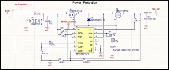
Schematics of the circuit we are currently using:

enter image description here

Any and all advice and recommendations would be greatly appreciated, as I am at wits end with this temperamental beast.

ocrdu
  • 8,705
  • 21
  • 30
  • 42
Hannes
  • 21
  • 3
  • 1
    Welcome! How does your layout situation look? What max voltage have you measured across it with your scope? What does the Vgs waveform look like on your scope? How much output current do you need? – winny Oct 03 '22 at 21:33
  • What current is flowing when the failure occurs? Can you verify compliance with SOA restrictions? – Spehro Pefhany Oct 03 '22 at 21:51
  • Sorry about my delayed response, I was in the process of moving house. We have failures at 40V using FDD86110 Mosfets (the same they use on their eval kit). We manage to complete a 80V test using STD85N10F7AG Mosfets but the load where the failure happens is at around 1.5W (using a programmable load). The testing is within the SOA for both Fets, and we have had pass on another board up to 15W+ using the same circuit, mys suspicion is layout, but other than the eval kit I can't find any board recommendations. – Hannes Oct 09 '22 at 20:47

1 Answers1

6

It looks like you've implemented the dV/dt moderation appnote slightly incorrectly with your D1/R4/R5/C6 configuration.

Schematic from the linked appnote

In the appnote, D1 is placed directly between \$V_{SUPPLY}\$ and the IC's gate pin. The 56Ω resistor and 1kΩ/220nF RC arrangement are only connected to the MOSFET gate.

In your circuit, you put the 56Ω resistor in series with both the MOSFET gate and the zener diode.

If you take a look at page 14 of the datasheet, it has this to say about operation beyond 35V:

With proper external component selection, the MAX16126/MAX16127's input voltage operating range can be extended beyond 30V. Normally the input voltage can swing up to 90V in protection mode, but normal operation is listed in the electrical characteristics table to 30V. Higher voltage operation is permissible so long as the resulting GATE bias voltage does not exceed 45V with respect to GND.

To enable operating voltages above 30V, a 6.8V Zener diode clamp can be added GATE-to-SRC to the external switches to limit the maximum GATE voltage. The circuit in Figure 4 shows the recommended arrangement. When VIN = 35V, VGATE = 35V + 6.8V or 41.8V. When VIN > 35V, the MAX16126/MAX16127 detects the input over voltage condition by sensing the voltage at the OVSET pin and turns off the charge pump. The resistive voltage divider on OVSET must be selected to disable the circuit before the gate voltage reaches 45V.

During normal operation the IC uses a charge pump to output a voltage at the GATE pin that is a few volts higher than \$V_{SUPPLY}\$, so that the \$V_{GS}\$ of the MOSFETs remains positive. The charge pump will continually increase its voltage as \$V_{SUPPLY}\$ increases. The maximum voltage allowed at the GATE pin is 45V above GND. The zener diode D1 is used to enforce this - when \$V_{GATE} - V_{SUPPLY} > V_Z\$, D1 starts to conduct and clamps \$V_{GATE}\$ to \$V_{SUPPLY} + V_Z\$.

You selected BZX384B10-G3-08, which is a 10V zener diode. As such you are allowing the GATE pin to reach all the way to 45V, which gives you zero margin. You should use a 6.8V zener diode here, as indicated in the datasheet.

Additionally, because you put the 56Ω resistor in the wrong location, a voltage drop forms across it which is added to \$V_Z\$. This means that the voltage at GATE becomes \$V_{SUPPLY} + V_Z + V_{R4}\$. Since \$V_{SUPPLY} + V_Z\$ is already 45V when \$V_{SUPPLY} \ge 35V\$, this is guaranteed to exceed the allowed maximum of 45V.
Polynomial
  • 10,562
  • 5
  • 47
  • 88
  • 1
    Thanks for that we will look, this design is based off the EVAL kit which was passing the testing, and reason for the chip selection. If you look at the layout on the eval kit, the resistors are in the right place, as per the two mosfet design, it also specifies 15V zenners, and which we dropped down to 10V for the reason you mentioned. I asked the lab to do a test using the 6.8V zener and the failure still happens at 40V drain. We have used this circuit successfully on another board, so my suspicion is its layout depended. I'll have another look at let you know once I'm back in oofice. – Hannes Oct 09 '22 at 20:54