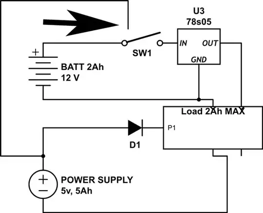
I want to prevent the +5 V from USB to reach the output (VO) of the 5 V-regulator of my 7.5 V battery. I tried to use a MOSFET (PNP) as shown in the image below but its not working. Any ideas?

I want to prevent the +5 V from USB to reach the output (VO) of the 5 V-regulator of my 7.5 V battery. I tried to use a MOSFET (PNP) as shown in the image below but its not working. Any ideas?
In your circuit, the MOSFET will switch on regardless of which power supply you connect.
When the 7.5V supply is not present and the 5V supply is connected to the source of the MOSFET, \$V_G\$ is 0V and \$V_S\$ is +5V. Therefore the voltage between the gate and source (\$V_{GS}\$) is \$V_G - V_D = 0V - 5V = -5V\$. A P-channel MOSFET turns on with a negative \$V_{GS}\$, so the MOSFET turns on, allowing current to flow between the drain and source, which means \$V_D\$ becomes 5V.

When the 5V supply is not present on the right, but the 7.5V supply is present, the voltage regulator's VO pin supplies 5V to the drain of the MOSFET. When the circuit is first powered on, the voltage at the source pin is 0V, so the \$V_{GS}\$ starts at 0V. Since \$V_D > V_S\$, the body diode conducts and a current flows across the body diode from drain to source. This causes the voltage at the source pin to rise.

After a very short time, the voltage at \$V_S\$ rises to the point where \$V_{GS}\$ exceeds the threshold voltage of the MOSFET, so the MOSFET switches on. Now current can flow between the drain and source, so the body diode is no longer part of the equation.

If you connect both supplies, you risk damaging your voltage regulator or causing an overcurrent condition.
The typical way to implement this kind of protection is as follows:
simulate this circuit – Schematic created using CircuitLab
This circuit causes the top supply to be used if it is present, otherwise it falls back to the bottom supply. This means that your external voltage supply will be preferred if both supplies are present.
In this design two MOSFETs are used back-to-back on each input. When the MOSFETs are switched off, their body diodes face in opposite directions to each other, so they block current in both directions instead of just one direction. Note that the MOSFETs on the left side (M1, M3) are oriented such that their body diodes oppose the flow of current from the supplies - this is important for the circuit's operation.
When SW1 is open (i.e. the external 5V supply is disconnected) the gates of MOSFETs M3 and M4 are pulled down to GND by R2. The gates of MOSFETs M1 and M2 are also pulled down to GND by R1.
The regulator is outputting 5V, so M3's \$V_{S} = 5V\$. As such, M3's \$V_{GS} = -5V\$, which means M3 turns on. This causes the voltage at M3's drain to rise. This pulls the gate voltage at M1 and M2 up to 5V, turning them both off. The voltage at M4's drain is now higher than the voltage at its source, so a current flows across its body diode, and its source pin's voltage rises to 5V. Since M4's gate is at 0V, M4's \$V_{GS}\$ is -5V, so M4 switches on too. At this point both M3 and M4 are switched on, and M1 and M2 are switched off. The load is fully supplied by the voltage regulator, and no current can flow "back" toward the external 5V input even if you short it to ground.
If you close SW1 (i.e. attach the external 5V supply), it pulls M3 and M4's gate voltages up to 5V. This causes their \$V_{GS}\$ to rise up to 0V or higher, turning both M3 and M4 off. Since M3 is no longer conducting, R1 pulls M1 and M2's gate voltages down to 0V. M1 turns on, because it has +5V at its source and 0V at its gate, making its \$V_{GS} = -5V\$. If the battery was present before the external supply was plugged in, the voltage at M2's source pin was already at +5V, so its \$V_{GS} = -5V\$ and it conducts immediately. If the battery was not present, then M2's source pin starts at 0V. When M1 switches on, M2's drain pin rises to 5V, so M2's body diode conducts and the source voltage rises to 5V. At this point M2's \$V_{GS} = -5V\$ and it conducts. This causes the load to be powered fully from the external supply, and no current back-flows to the regulator or battery.
You can accomplish your goal with a small change to your circuit. Connect the output of your regulator to the P-MOSFET gate. Place a Schottky diode between the gate and source. Connect the USB voltage to the drain. Your voltage output for the circuit is taken at the source.
As long as your regulated voltage is > USB-side voltage + diode drop + Vgsth, the MOSFET will be OFF. If less, the MOSFET will be ON. Regardless, the Schottky prevents current flowing from the USB to the regulator output. The body diode will block current flow from the regulator output to USB. Ideally, you'd have a regulated output such that Vout is always > USB (5V) + diode drop + Vgsth so the MOSFET always OFF when both the battery and USB are present.