2

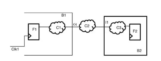
Consider the following circuit in an FPGA:

enter image description here

Let's say the output port O1 is constrained to have a min/max delay of 1 and 3 ns respectively. That means the circuit will be optimized for allowing a max. of 3 ns delay, after the Clk1 trigger, from F1/D to O1.

This will have an impact on the input delay constraint at I1, right? I mean, if the max. output delay at O1 is constrained to 3 ns, and the sum of all the rest of delays until I1 (wires, C2...) is constrained to, say, 10 ns, then the maximum input delay at I1 will need to be constrained to 10+3=13 ns, right?

If this is correct, why do I need to specify the input port delay at I1 if it can be inferred from the max. output delay at O1 and the max. delays from O1 to I1 (wires, C2...)?
Martel
  • 1,213
  • 6
  • 20
  • 1
    Didn't you ask this question yesterday? Please don't delete a question and re-ask the same thing. – Hearth Sep 18 '22 at 15:40
  • The input/output delays are used to constrain inputs and outputs of FPGAs. Do you have 2 different FPGAs on your block diagram? –  Sep 18 '22 at 16:28
  • Don't you confuse input/output delay and min/max delay? Or I misunderstand your issue –  Sep 18 '22 at 16:30
  • What is the clock of F2? –  Sep 18 '22 at 16:31
  • @hearth I asked a question way longer that was split in input and output port delays, but specially it was longer and treated at least 2 more topics other than this one. I want now to ask about this in particular. I don't see anything nothing wrong to delete a question that has not been answered yet in order to ask something more concrete and concise. – Martel Sep 18 '22 at 16:56
  • @gotchi85 The book I'm using doesn't mention 2 different FPGAs, I imagine the figure corresponds to 2 different blocks inside the same FPGA. Although I have tried the VIvado constrains wizard and it mentions that input/output delays are for FPGA boundaries, so you might be right. – Martel Sep 18 '22 at 16:58
  • @gotchi85 The book doesn't mention the clock of F2, but I think that it must be a different one from Clk1. Do you mean that this is determinant because for an output port delay will use the clock of F2 as reference? – Martel Sep 18 '22 at 17:01
  • @Martel Ah, okay. In that case, that's fine. I didn't recall what all the other question was about. Might have been better to edit the original question, but I don't think there's much of a problem here. – Hearth Sep 18 '22 at 17:06
  • @gotchi85 With regards to the confusion about the input/output and max/min delays, do you mean that input/output port delays affect only to FPGA boundaries (ports that come from, and leave to, literally outside the FPGA chip)? If that's the case, the input/output port delays are not applicable at all for inputs/outputs of modules within the FPGA? – Martel Sep 18 '22 at 17:07
  • 1
    I guess comments are not the right place to post an answer. Input output delays are for FPGA boundaries and not inside submodules. Min and Max delays are for paths inside, often used in clock domain crossings for example –  Sep 18 '22 at 19:28

1 Answers1

1

As explained by @gotchi85 in the comments, input/output port delays apply only to FPGA boundaries. In other words, B1 and B2 would be different devices in the example above (being the FPGA one of them).

Having said this, if the FPGA is optimized to compensate the input/output delay, this indeed will relax the requirements for the input/output device.

Martel
  • 1,213
  • 6
  • 20