2

The transistor configuration found in the schematic below can be used as the input to an op-amp that can work with a common mode input at or above the high supply rail. For example this configuration appears in the design of Analog Devices' LT6015 "over the top" op-amp IC. Does this transistor topology have a name?
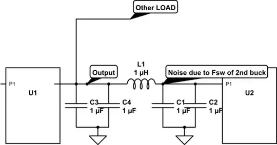
schematic

simulate this circuit – Schematic created using CircuitLab

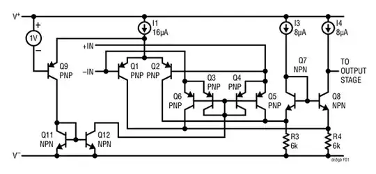
The circuit consists of two current mirrors: Q1 and Q3 and Q2 and Q4. Assuming the current mirrors reflect current 1:1, and neglecting the base currents which are small in comparison to the collector currents flowing in Q1 and Q2, the sum of the output currents is equal to the reference current. If the majority of the reference current gets divided equally between the collectors of Q1 and Q2, then the output currents will be equal. However, a difference in the input voltages will cause the reference current to be divided unequally between the current mirrors, and will result in unequal output currents.

For reference, here is a stylized schematic from the LT6015 datasheet.
enter image description here

Math Keeps Me Busy
  • 18,947
  • 3
  • 19
  • 65
  • Math, just look at it. Q3 and Q6 make up a current mirror. Q4 and Q5 make up a different current mirror. A difference between them is where the emitters are tied. So any difference in the +IN and -IN means a difference in their collector currents, which are coupled to the long tailed pair of Q1 and Q2. Think about what this means. – jonk Sep 07 '22 at 13:39
  • @Jonk. I understand how the circuit works. If I had to name it myself, I might name it something like differential current mirrors. But there are configurations like "Widlar current source" or "differential pair" that have specific names that are recognized by "everyone". I'm wondering if this configuration has a name, or whether it is just "a pair of current mirrors combined in a way to accept a differential input voltage"? – Math Keeps Me Busy Sep 07 '22 at 13:47
  • @MathKeepsMeBusy I think it's just a current mirror, in the same way a mutiple collector/emitter transistor in the same configuration would be just the same. It would just look weird from a "usual" circuit's perspective (e.g. breadboard). In fact, the more I look at it, the more I think those *are* a multiple C/E thing, and this is just another graphical way of showing it. But then, I can't really say this for sure. – a concerned citizen Sep 07 '22 at 14:08
  • @MathKeepsMeBusy I don't think the limited section you pulled out has a name. Coupled into the circuit, it may, as then it has meaning to me. Not pulled out as you did, though. Then it seems meaningless and undeserving of a name. But I don't care much about the names of things unless there's a communication need. And in this case, I think the communication need would only come from the larger topology. Not the tiny piece you pulled out. That said ... who knows? Maybe someone will find a name for you. I'm clueless about that. – jonk Sep 07 '22 at 14:11
  • @Jonk, communication is why names are useful. In some cases I want to say "use a differential pair" without having to explain exactly how a differential pair works. If I want to use this circuit, say in a circuit for an "ideal diode" (not the op-amp kind, but the power circuit kind) I would be nice to say "use a ____" without having to give the details of how the circuit above is wired. I imagine linear IC designers would have need for such names, and might be able to give such a name, but maybe not. – Math Keeps Me Busy Sep 07 '22 at 14:27
  • @MathKeepsMeBusy Never said communication isn't useful. But I don't care about that for understanding a schematic, since there's no human involved. That's all. I don't believe there's a specific name for this "piece" you call out because I don't think it stands alone well enough by itself without the surrounding Q1+Q2 pair's topology. But of course I may be wrong. – jonk Sep 07 '22 at 19:30

0 Answers0