2

Schematics

enter image description here

The datasheet of SE2305Q is HERE

I have an LCD screen that comes with a backlit_power pin which requires 3.3 V to light up. It draws quite some current, and I don't think it is good practice to directly connect it to the microcontroller.

Instead I used this P-channel MOSFET to act as a switch. Since the screen only provides a power pin for the backlight, I don't think there is a simple way to use an N-channel MOSFET.

All connections are to common ground.

The problem is no matter the signal is 0 V (which Vgs is -3.3 V) or 3.3 V (which Vgs is 0 V), there is no action on the drain. Basically, it does not turn on the LED.

Can anyone point me in the right direction?

Simeng Fu
  • 23
  • 3
  • First, be certain that you know how the BACKLIT_LED input behaves. With a DMM set to measure current, measure current between BACKLIT_LED and 3.3V. – Mattman944 Sep 01 '22 at 13:17
  • 1
    Also, check what the MOSFET drain voltage is when the gate voltage is pulled low. Your schematic looks correct and the MOSFET selection is fine. – 65Roadster Sep 01 '22 at 14:14
  • Thanks for your reply! I have checked the voltage: when Gate is LOW (0v to ground), Source is 3.3v to ground, Drain is 0v to ground, Gate to Source is -3.3v (positive probe to Gate), Gate to Drain is 0v (positive probe either pin), Source to Drain is 3.3v (positive probe to Source)..... BACKLIT_LED works fine if I connect it directly to 3.3v. Very Strange behavior. – Simeng Fu Sep 01 '22 at 15:06
  • Your diagram looks correct, although you will get more people to help if you draw a proper schematic (3.3V on top, flow left to right, MOSFET schematic symbol). Maybe post a picture that shows the connections so we can double check the pinouts. – Mattman944 Sep 01 '22 at 16:50
  • @Mattman944 Sure, I understand that this drawing is not according to the standard, it is a web editor that provided by the part supplier which I use to find parts and organize BOM files, it is not that professional for schematics designing but saves quite some trouble to get PCB manufactured. Thanks for point it out! Do you mean a picture of the PCB or ....? – Simeng Fu Sep 01 '22 at 17:43
  • 1
    They may have interchanged gate and source in the datasheet because typically gate is at pin 1. You can try to find the body diode to be sure. – Jens Sep 01 '22 at 17:43
  • @ Jens. Oh! I am for sure will check that out. Thanks for the heads up! – Simeng Fu Sep 01 '22 at 18:04
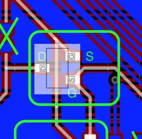
  • Your layout has the standard connection scheme for gate and source, the datasheet shows a different one. Your schematic doesn't match your layout. – Jens Sep 01 '22 at 18:44
  • @Jens. Sorry, forgot to mention that the layout is a "top view" and the layout is the backside, so what you are looking at is the bottom side of the mosfet. the layout is automatically generated by the schematic, and I double checked that the pin numbers match the schematic. sorry I forgot to mentions this earlier. – Simeng Fu Sep 01 '22 at 18:54
  • The datasheet g and s are swapped from the large majority of SOT23 FETs. Whether this reflects reality is TBD. – ATCSVOL Sep 02 '22 at 01:21
  • I can confirm that the pins are swapped. It is a fault of definition of the component symbol in the editing software. I rewired MOSFET and now it worked nicely. Thank you all for your help, I don't know how much energy that I would have put in to solve this without your help since all my attention are focused on faults that might be in my schematics. – Simeng Fu Sep 02 '22 at 06:58

2 Answers2

4

Sorry per the first data sheet I found it will not work, the Vgs of that MOSFET was stated at 4V. If that is correct you need a different one with a Vgs of about 2V. There were several datasheets and they are not all the same. I found another data sheet that says it is a good choice. This is that link: https://datasheetspdf.com/pdf-file/1419927/WILLAS/SE2305GD/1. Check the threshold and Vgs for the part you have. It appears you either have a mislabeled or bad part.

Most manufacturers use different processes hence there part will not be exactly the same as another etc. They process them to a given recipe then after test to there defined parameters then label them accordingly. It is also very easy for an unscrupulous person to put whatever identification they want on them. This has been a big problem in the semiconductor industry for many years.

The reason I say this several others and myself know what you have is correct even if not technically drawn to a specific drawing standard. I do not know your supply chain and its sources. Hopefully it is a reprutiable reseller. Not all of the counterfeit parts come from china but many do.

Gil
  • 4,951
  • 2
  • 12
  • 14
  • Thanks for your effort! So basically this is because of a unsuitable mosfet? I did not find 4V as Vgs can you be more specific? The datasheet is provided by this manufacture from whom I accquited these mosfets. The model number is the same on the datasheet. I am a bit confusing. – Simeng Fu Sep 01 '22 at 19:03
2

Datasheets show the top view unless otherwise specified. Pins are normally numbered counter-clockwise.

So, assuming that your PWB view is from the top, you have the pins wrong.

enter image description here

Mattman944
  • 13,638
  • 1
  • 19
  • 43
  • Thanks! I will swap the pins with conductive paint and report back! Thanks for your help. But it is weired that the layout is auto generated according to the schematic...maybe there is an mistake in the pin definition in the supplier's database. Anyway, I will swap the pins to see if it solves it. – Simeng Fu Sep 01 '22 at 20:23
  • I can confirm that the pins are swapped. It is a fault of definition of the component symbol in the editing software. I rewired MOSFET and now it worked nicely. Thank you for your help. – Simeng Fu Sep 02 '22 at 06:55