I have searched for weeks on the internet but it seems SMD devices have no fixed rules- anyone can name any chip any number/letter! No result searching this forum either.
I am trying to identify a few SMD components to draw a schematic and repair a circuit that drives a VFD (vacuum Fluorescent Display).
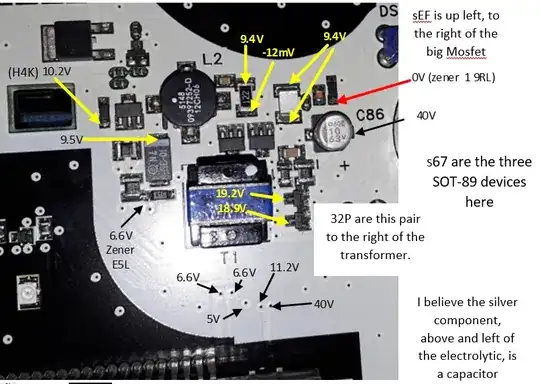
32P is an SOT-23 (I think) 3-pin device. I assumed it was a transistor but now I wonder.
s67 is a 3-pin plus tab device that I believe is a transistor (or Mosfet?). I think it looks like a SOT-223 but the tab doesn't seem to bend down; it looks like it is flat, so maybe SOT-89.
E5L, H4K and 1 9RL are 2 contact devices (look like SOD-123 and I think zener diodes).
The E5L has 6.6V at the cathode and it never varies, so it does seem it's a zener (has a resistor from positive rail to the cathode then the cathode leads to two pins of a VFD (Vacuum fluorescent display). The H4K is arranged the same way and has 10.3V at most, even when I increase the input voltage to the circuit, so again seem to be a zener.
The 1 9RL (it looks like a space between 1 and 9, but maybe that's not significant) seems to be a zener too and arranged the same way. When the circuit powers on there is no voltage on the cathode, so the cpu it connects to must be pulling it down. I removed it from the PCB and tested it on a PSU with a limiting resistor. It topped out at 5.6V so seems to be a 5.6V zener?
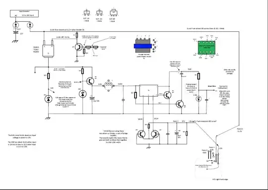
So far the rough schematic I drew doesn't make full sense and I haven't spotted any problem that would solve the fault. Can anyone help? It's driving me mad.
Note: In the dark, the VFD has a dim pink glow on the front cathode wires while turned on. As the display turns off, some of the characters blink in normal green brightness for a fraction of a second. It would seem the voltage biases fall through the correct levels for a split second.
Aug 23rd: Thanks Jens. I just saw your diagram. This makes sense now of what is on the PCB and what I was looking for. Yes, I was wondering if the 32P devices were forming a rectifier, but could not find any components on the internet named 32P. Clearly you have seen this type of circuit before :) and know how the transformer windings should be.
So the components I was wondering about would seem to be Ok, from what you have say.
I have redrawn my schematic to incorporate your insights.

I suppose that answers my original question and so I cannot get any other help on this then (?).
Oh well, thank you very much for showing me what the schematic should be and how it works. I appreciate this. I will soldier on and try to think of what I can try next. Maybe there is a more suitable forum area for VFD problems. My next thought is why doesn't the 37V appear on at least one of the VFD pins. Or is it normal for the 37V to go to the driver ICS (as I have already checked) but maybe the driver ICS have failed? Also, I need to figure out why the 5.6V at the zener is held down to zero and if that is by design or fault. I have nothing else to go on except that the VFD did operate dimly when I got this instrument panel and then stopped showing anything.
Thank you again for moving me a stage further.


