0

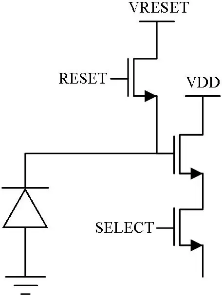
This is a standard pixel circuit:enter image description here It works just like one would expect. When the reset signal on the gate of the PMOS is low it is conducting and charges the capacitor to 5V, then when the signal turns high it stops conducting and the capacitor is slowly discharged by the current source and its voltage is forwarded to the output by the two NMOSes. This gives an output swing from 4V (since there is a 1V drop across the source follower) down to 0V.
My problem is that the PMOS takes large area on an IC so I would like to replace it with an NMOS as well.

The simplest solution would be just to replace it as it is:enter image description here However, for some reason the capacitor in this configuration doesn't charge up to 5V only to about 4,2V losing almost a volt on the output range. Can someone explain what is the reason for this?

Another solution could be turning the circuit upside down:enter image description here This seems to work well but I've noticed that the capacitor charges up slower than it discharges in the PMOS circuit giving a slightly different characteristic. I would like to know what is the reason for this difference.
The circuits that appear on the internet seem to be using the first NMOS configuration but with a different drain voltage than Vdd:

enter image description here

Why is this the ideal setup, why is it better than my suggestions, and what would be a suitable voltage for Vreset?
  • You really shouldn't be using discrete 3-terminal MOSFETs for IC design. Unfortunately, Falstad and CircuitLab don't have 4-terminal MOSFET components. However, there are free simulators such as LTspice, ngspice, and Micro-Cap which do include this functionality. – Ste Kulov Aug 12 '22 at 13:56
  • These are 4 teminal mosfets, aren't they? Bulk is shorted to source for all of them. – Ching Chung Aug 12 '22 at 14:04
  • @ChingChung Unless you have isolated wells, FDSOI, or other shenanigans, all of your bulks are shorted *together*, not to individual sources. That common bulk substrate typically connects to VSS, while the substrate of the pFET's nwell often connects to VDD. I'm also curious about the 22 nF capacitor - you're worried about space, but 22 nF in MIMcap or even MOMcap realizations is going to take a lot of area. – nanofarad Aug 12 '22 at 14:47
  • What is a "standard pixel circuit"? What's the pixel? What is the circuit supposed to do? – Kuba hasn't forgotten Monica Aug 12 '22 at 15:07
  • @nanofarad that is just the junction capacitance of the photodiode used for the simulation exclusively. It is not an actual component. What size capacitors would you say can be practically produced on an IC? – Ching Chung Aug 12 '22 at 15:08
  • @ChingChung Ah, PD junction capacitance makes more sense. As for on-chip: tsmc 65nm mixed signal can do 2 fF/μm^2 (public number from MPW provider). Intel 10+ did much better and claims 30-50 fF/μm^2 (not sure if any performance tradeoff, source is https://doi.org/10.1109/IRPS45951.2020.9128312). – nanofarad Aug 12 '22 at 15:36

1 Answers1

1

However, for some reason the capacitor in this configuration doesn't charge up to 5V only to about 4,2V losing almost a volt on the output range. Can someone explain what is the reason for this?

This is what happens when you use an NMOS to replace the PMOS in your circuit. The NMOS acts as a source follower and, the voltage at the source will be hundreds of millivolts to several volts below the reset signal level at the gate. If you want to use an NMOS there your gate reset signal has to rise several volts above the 5 volt rail.

Another solution could be turning the circuit upside down. This seems to work well but I've noticed that the capacitor charges up slower than it discharges in the PMOS circuit giving a slightly different characteristic. I would like to know what is the reason for this difference.

The only issue I see is that the NMOS source isn't connected to ground but to +1 volts.

Why is this the ideal setup, why is it better than my suggestions, and what would be a suitable voltage for Vreset?

I can't really say anything about this because the circuit aims are not defined.

Andy aka
  • 434,556
  • 28
  • 351
  • 777
  • Thank you, you are right in terms of the source follower. For the second circuit the source needs to be connected to 1V to keep the gate-source voltage of the top right transistor above the threshold voltage. Meanwhile I have noticed that a slight difference between the pmos and the second nmos circuit is that the bottom right transistor starts out in saturation with the pmos and linear in the nmos version. Could this be the reason for the difference? And the goal is to create a similar performin nmos version of the pmos circuit without increasing the complexity too much. – Ching Chung Aug 12 '22 at 14:00
  • 1
    I think signal level graphs from a simulation would help you resolve this difference. I would however recommend a decent simulation package like micro-cap though. – Andy aka Aug 12 '22 at 15:28