8

I am making a boost converter for a Geiger counter, based on the STM8L152 MCU. Here's the circuit:

enter image description here

The circuit reaches the correct voltage and consumes only 8 μA, however, there are parasitic oscillations in the comparator output (yellow trace), and I'd like to get rid of them to reduce consumption even further.

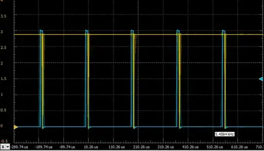
Apparently, these oscillations are caused by VREF level changes during every comparator output transition (VREF - blue trace), since VREF is smooth when the comparator output is constant.

VREF ripple Yellow trace - comparator output, Blue trace - VREF ripple

Even though VREF output buffer in the MCU is very weak (max output current - 1 μA), I don't see what could be the reason its ripple is so high, -- the comparator has a 1 pA bias current, there's no way it can create so much load on VREF.

I've tried bypassing VREF with a 0.01 μF cap, this decreased VREF ripple to ±1 mV (which I think is a lot for such a large capacitor). What's even worse, it caused a 14x increase in current consumption (110 μA with bypass, 8 μA without it) and a slight increase in output voltage (105 vs. 95 V).

With VREF bypassed, the converter sends a lot more pulses to the transistor than it does without bypassing. Here are TIM1_CH2 outputs for both cases:

enter image description here

TIM1_CH2 output, no bypass on VREF

enter image description here

TIM1_CH2 output (blue trace), VREF bypassed with 0.01 μF

Obviously, much more frequent switching is causing increased power consumption but why does it switch more frequently with smoother VREF in the first place?

If anyone wonders why in the first case parasitic oscillations are not getting into the timer output, they get filtered out by a 8 kHz input filter inside the MCU.

How do I get rid of the oscillations and get low power consumption? The only idea I have is adding more hysteresis but at the moment I don't have high-value resistors to implement it.

UPD: Adding board photos and layout as requested:

UPD2: Antonio51's answer seems most promising so far. Adding a 15 pF capacitor from comparator's IN- to ground reduced power consumption to 12 μA. I'll experiment with the capacitor values, I think increasing its value should bring the pulse bursts to low enough frequency (and thus low power), just need to find the sweet spot between output ripple and power consumption.

enter image description here

enter image description here

Archimedes
  • 585
  • 4
  • 10
  • 3
    It is interesting that your 2nd trace (pulsing @ 5.4584 kHz) is a 3rd subharmonic of MCU's 16.4 kHz clock source. I'm imagining either electromagnetic coupling or GND-current coupling into that comparator. Your voltage divider's *very high* resistance values might also be a problem...a 12Meg resistor is NOT 12Meg for those fast switching transient edges. – glen_geek Aug 01 '22 at 14:42
  • 2
    It seems to me that 1 G Ohm and 12 M Ohm are a bit too "high", especially when adding "parasitic" capacitors. – Antonio51 Aug 01 '22 at 14:54
  • Your comparator's inputs can process voltages 0.3V above the supply voltage. Why not use the 1.8V supply as reference then? perhaps you'll need to RC filter it, but it will have much lower output impedance than VREF... – bobflux Aug 01 '22 at 16:53
  • 2
    The circuit diagram does not agree with the actual circuit layout. Please show the diode doublers and all that other funk. It does actually matter. When a circuit doesn't work, you usually don't know what's important and what isn't, so it really saves everyone's time to post everything you got, including a full schematic. – Kuba hasn't forgotten Monica Aug 01 '22 at 20:01
  • The answers given below cover many issues that may be responsible, but I'll add another suggestion. Use a MOSFET for the switch, and appropriate gate resistors. And, as has been suggested, provide a complete schematic along with actual part numbers, component specifications, and design parameters. – PStechPaul Aug 01 '22 at 21:19
  • 1
    The board layout seems to show the 10 mH inductor connected directly to Vcc and the collector of the transistor. The schematic shows a 130 ohm limiting resistor. Also, although the comparator has only about 1 pA input current, internal parasitic capacitance can cause considerable transient noise on the inputs, which may be why there is ripple on the Vref input. – PStechPaul Aug 01 '22 at 21:38
  • @PStechPaul yes, it is connected directly to VCC, 130Ω is series resistance of the inductor, for quick reference and simulation purposes. Also good luck getting a 100V+ MOSFET that will have low Rds at 1.8V gate voltage :p – Archimedes Aug 02 '22 at 23:01
  • This is characterized on 2Vg: https://www.mouser.com/ProductDetail/ROHM-Semiconductor/RD3S100CNTL1?qs=W0yvOO0ixfG07%2FCx8fGFxA%3D%3D 190V 182 mOhms https://www.mouser.com/datasheet/2/348/rd3s100cntl1-e-1873145.pdf https://www.vishay.com/docs/68642/sia456dj.pdf 200V 3.5 Ohm at 1.8 Vg (Non stock) I guess you are right. – PStechPaul Aug 03 '22 at 00:28

3 Answers3

8

The circuit reaches the correct voltage, consumes only 8uA, however there are parasitic oscillations in the comparator output

There will always be some oscillation here because the MCP6541 comparator you have chosen has an internal hysteresis of a few millivolt and, this will keep the circuit over-shooting a little bit and then undershooting a little bit.

It's normal behaviour for this type of circuit.

Apparently, these oscillations are caused by VREF level changes during every comparator output transition

It's likely that the reason Vref changes is because of the inevitable ripple voltage on 1.8 volt power rail and, this is also influencing the power rail for the MCU. I don't think it can be the comparator causing this. Have you tried putting a bulk capacitor on the boost power input to provide a local energy source. What sort of power rail decoupling have you implemented on your MCU?

Andy aka
  • 434,556
  • 28
  • 351
  • 777
  • There is a 47uF low ESR electrolyte cap and 1uF ceramic on the board and 0.1uF ceramic near each chip. Initially there was only the 1uF ceramic, adding aforementioned capacitors made no difference. Peak inductor current is only 4mA, and I don't see any ripple on power rail. – Archimedes Aug 01 '22 at 13:59
  • > "some oscillation". Yes, some oscillation. When signals are very close to each other. But here I'm getting a steady 35-ish kHz oscillation. Too bad I can't test now if increasing hysteresis will help. Massive VREF ripple is still a problem too though, not sure how to fix it too. – Archimedes Aug 01 '22 at 14:02
  • @Archimedes maybe you should add the PCB layout to the question? Maybe add a 10k resistor in series with the Vref line to the comparator to see where the disturbance comes from? – Andy aka Aug 01 '22 at 14:24
  • @Andy_aka, done – Archimedes Aug 01 '22 at 16:02
  • 2
    It looks like it could be a layout issue and a wiring issue to be honest. The lack of a decent ground plane on the circuit could also make measurements problematic and, those weakened measurements could be made worse by poor oscilloscope probing. Not being able to identify the ICs on the board is not helping. – Andy aka Aug 01 '22 at 17:18
  • I do admit poor layout, though I have doubts that it influences circuit performance *that* much. The board does have some sensitivity to my body and mains wires but I have to put the board really close to the EMF source for a significant impact on performance. Still, I'll remake the board to have a ground plane and a direct connection to the MCU board, without wires. I also updated the board and schematics, hope it's more clear. The board is populated only with components shown on the schematic. – Archimedes Aug 02 '22 at 22:59
  • @Archimedes with any circuit like this, you have to get the layout right and have voltage references local. This needs to be fixed. Even if you want to use the MCU's voltage reference I would place a local voltage reference on the little PCB so you can prove to yourself that it is the wiring that caused the Vref problem. – Andy aka Aug 03 '22 at 06:49
2

With VREF bypassed, the converter sends a lot more pulses to the transistor than it does without bypassing. Obviously, much more frequent switching is causing increased power consumption but why it switches more frequently with smoother VREF in the first place?

Without the VREF bypass, the circuit doesn't maintain good regulation at all. It is sluggish. So it generates the pulses less often. The pulse packets act like a single longer pulse, since the inductor filters them and only "sees" their average, more-or-less.

With the VREF bypass, it actually works as designed, and the current consumption is what's needed to keep the output voltage within the hysteresis window. You did nothing to control the frequency of the pulses, so what you got is what the circuit should be doing. If you want it to do something else, then you have to change the design.

You don't have the instrumentation to measure the output voltage ripple on this circuit, since you can't just clip a scope probe there, or even a DVM. A DVM has 10Mohm input impedance - completely defeating the point of the 1Gohm feedback resistor. You'll have to add a JFET or CMOS buffer op-amp to the feedback divider node, so that you can observe the output voltage level without loading stuff down into oblivion. Then you can compare the ripple with VREF bypass and without it. You'll observe that the output ripple without the bypass will be worse, I expect, and that the circuit is in fact regulating much better with the VREF bypass.

When you'll be slowing the pulse rate down, you'd be trading off ripple for current consumption. How much of a tradeoff you allow must be actively controlled either by changing the comparator hysteresis or by limiting the pulse rate out of the timer (the pulses should be gated to occur less frequently).

Finally, the high-impedance node has no shielding and no guarding, and the relatively large loop areas likely magnetically couple into the high impedance node, and probably also into the VREF node.

the comparator has 1 pA bias current, there's no way it can create so much load on VREF

The 1pA comparator bias DC current is nothing much compared to the leakage current due to surface board contamination as well as currents induced into the VREF trace, never mind capacitive coupling. For impedances you're using, the board looks filthy. It must be cleaned from all flux, using a suitable flux remover, and then cleaned from ionic contamination with deionized water. Then it should be dried and not touched with bare fingers.

The high impedance node could use at least AC guarding: a guard trace connected to ground but also AC coupled to VREF. So you'll need to keep the VREF decoupling for that.

The 1.8V - inductor - transistor - ground AC current loop need to be as tiny as practical. The source of the AC current would be the decoupling capacitor, which should be right next to the inductor, right next to the transistor, and the transistor's emitter must return right back to the decoupling capacitor.

Same goes for the 1.8V - inductor - transistor - diode - output storage capacitor - ground loop.

The layout at the moment is very loosey-goosey. These components in the fast current loops need to be tightly spaced, and should be sitting on top of a ground plane as well.

The transistor is driven into saturation, so it turns off relatively slowly compared to how fast it turns on. You probably should make both switching events balanced, since those will affect the losses somewhat, but also will affect how much the current transient couples into the sensitive nodes. Since you seem to be OK with turn-off from saturation, make the turn-on similarly slow. You'll thus want to add a current-sense resistor into the inductor loop, and a fast instrumentation amplifier to condition the signal, so that you can observe it on the scope along with the output voltage and control signal - that way you can judge whatever changes you implement to slow down the switching.

The unloaded HV output current, with just the feedback network connected, is about 0.1uA, so the average inductor current is about 5uA, and the IIR losses are acceptable, so at least that's OK. Of course, as soon as you connect the diode multiplier etc., the inductor current will go up. I'm not sure how much leakage there is through the multiplier and how much current a Geiger tube needs in a background radiation environment, but those must also be kept in mind and you should be able to measure them. Thus - there should be a current sense resistor in the return leg of the HV circuit. I suggest using wideband amplifier for the current monitoring, since it helps to detect corona discharge - a rather fast pulsed phenomenon.
  • I have an electrostatic voltmeter with 100GΩ input impedance, and it has enough resolution to show if ripple is within acceptable margin. And it is. In fact, I can have quite a lot of ripple since at 400V a pulse from Geiger tube has 50V amplitude, so it's easy to distinguish it from ripple. Lowest possible power consumption is my goal here and I can trade a few volts of ripple for a few microamps of consumed current. – Archimedes Aug 02 '22 at 22:49
  • I do admit that my board is a bit crude and I was lazy to make a double sided board with a ground plane, I will remake the board to have a ground plane and use direct connection to the board instead of wires. Also I'd disagree about the cleanness, I've used plenty of flux cleaner and there is a huge cutout underneath the 1G resistor. If there were leakages in the feedback loop, the output voltage would be lower than expected but I get exactly the voltage I've calculated, within component tolerances. – Archimedes Aug 02 '22 at 22:49
  • Regarding capacitive coupling, I do admit this might be the issue but if you calculate the kind of capacitance and leakage that causes VREF ripple, you'll get impossibly high leakage and capacitance even for this board (or is it just me doing the numbers wrong?). Plus I'll be adding a small smoothing cap into the feedback as Antonio51 suggested, which will reduce coupling effects even further. – Archimedes Aug 02 '22 at 22:52
  • And about the transistor/inductor part. It is supposed to be driven by a 16.4 kHz, 50% duty oscillator. This is plenty for the transistor to open and close and my goal is to make the feedback loop provide long enough gating pulses for oscillator to stay on for at least a few oscillator cycles. With VREF decoupled this is not the case thus increased losses. What do you mean by balanced switching events? – Archimedes Aug 02 '22 at 22:53
  • Measuring inductor current is not a problem too, I have an equation for the boost converter, I can easily get consumed current from transistor base driving waveform. Equation will not work if pulses are too short but again, the ultimate goal is to avoid this mode of operation. – Archimedes Aug 02 '22 at 22:53
  • @Atrchimedes When measuring current, you have to actually measure current. The equations only apply when the circuit is working as you imagine, and it clearly isn't. So measure current with current shunts, directly. – Kuba hasn't forgotten Monica Aug 06 '22 at 00:15
1

If you want a good "transmission" of the attenuator (unless it is wanted so) ...
or "compensated" attenuator ...

Don't forget this :

enter image description here

If you change the capacitors, you should not expect what really is wanted.

EDIT: Ok, I can't reproduce exactly your circuit.
I am trying simply to explain that this problem can affect the comparator behavior.

The DC value can be ok if it is filtered.
If not, AC will affect the comparator seriously ... because the ripple on the output is transmitted quasi integrally to the comparator (here factor is quasi 0.5, parasitic capacitor of 5pF each).

enter image description here

To avoid this effect of AC perturbating pulses, do a compensation as what we do on scope probes.
Add perhaps a little capacitor (parallel on R1, 1 or 2 pF ... 200V min), and add for just a short time a "variable" capacitor C2 on R2.

Square wave generator on top of R1, scope at Vo (NB: remember, probe x10 -> parasitic capacitor added ~ 7 pF). Change value of C2 until good square on screen.
Subtract then "probe capacitor" ... "compensation" done for R1 & R2.

NB : Common-mode Input Impedance ZCM — 10^13||4 — ||pF
.........Differential Input Impedance ZDIFF — 10^13||2 — ||pF

You can also add ("brute force") progressively capacitors on R2 until all is good.

Antonio51
  • 11,004
  • 1
  • 7
  • 20
  • 1
    Not sure how this is supposed to help in my case, this divider is intended for AC signals, I'm working with DC here – Archimedes Aug 01 '22 at 16:03
  • 1
    Yes, voltage divider is DC. The MCP6541's low bias current has encouraged you to use very high values in the voltage divider in an effort to aid your low-power requirement. But 11Meg input impedance to a comparator is asking for trouble. The extra capacitance from comparator input to GND that Antonio51 suggests may help lower impedance here. Carefully choose the GND point for C2! One tries these tricks - depending on the source of undesired feedback, it may make things worse. – glen_geek Aug 01 '22 at 17:01
  • Hum ... The problem is not the DC voltage, but the AC part of the output voltage which is probably made of "fast transitions" on the capacitor of 10 nF ... So the divider depends also of the AC which "modifies" the DC ratio. I will add in answer what I "mean". – Antonio51 Aug 01 '22 at 18:15
  • I've tried adding C2 = 15pF and it significantly decreased power consumption, down to 12uA. Adding C1=10pF decreased it further, down to 9uA. We're almost there! Your solution seems most promising so far, I'll do more testing later. Can you elaborate on C1? I've seen feedthrough capacitors being used in DC-DC converters but I don't understand how exactly they help in my case since they pass AC and my goal is to trigger the comparator as infrequent as possible. – Archimedes Aug 02 '22 at 17:00
  • Ok. Note that C1 can be chosen by yourself as little as you want (including 0 pF added, but remember the fact that the resistor 1 G has its own "parasitic" capacitor). C1 can be evaluated and another "little" capacitor can be added (some pF). C2 must be added until R1xC1=R2xC2. – Antonio51 Aug 02 '22 at 17:17
  • Ok, it must be difficult because you don't know this little C1 value, but don't care really. Just add C2, square generator on top of C1, and see the result (with a scope) of varying C2 until you see a "good" square at Vop. (same as you make a "compensating" probe on a scope. Then "subtract the value of the x10 probe, generally 7pF). That's all... Good luck. Will add also it in my answer. – Antonio51 Aug 02 '22 at 17:17
  • The scope of C1 (not well known) is to make "easier" the "compensation" ... ie the "attenuation" factor for R1 & R2 (DC) which should be the same for C1 & C2 ... so it is "wideband". So, pulses on Vo are attenuated also exactly as DC. – Antonio51 Aug 02 '22 at 17:32
  • Remember that the input capacitor (some pF) of the op-amp is part of C2. – Antonio51 Aug 02 '22 at 17:36
  • So C1 on your schematic is just a parasitic capacitance of the resistor, not an actual capacitor? – Archimedes Aug 02 '22 at 18:21
  • Right for C1. If you have some "difficulties" with C2, you can add some "0.1 pF" to "C1". Remember choosing the right "voltage" ... – Antonio51 Aug 02 '22 at 18:53
  • Curiosity ... Common-mode Input Impedance ZCM — 10^13 Ohm **|| 4 pF** , Differential Input Impedance ZDIFF — 10^13 **|| 2 pF** . – Antonio51 Aug 02 '22 at 18:59
  • With C2=47pF I've managed to achieve 8uA consumption with little ripple. The circuit now operates as I wanted it to. I doubt that I'll get less than that with the inductor and transistor I'm using here. Your solution is actually straightforward and intuitive, I'm a bit ashamed I didn't come up with it myself. – Archimedes Aug 03 '22 at 12:44
  • 1
    No worries and no shame! Nobody is "perfect" ... and sometimes, we forget ... or don't find the right idea ... immediately. – Antonio51 Aug 03 '22 at 15:49