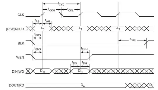
I have designed a simple internal SRAM memory where I initiate the write enable and read enable via DIP switches.
Verilog input wire has been declared in the simple memory read write which connects to these DIP switches on an external breakout. The program is currently not working in this setup.
My question is if giving external DIP switch for WEN and REN signals is a good idea?
Some more details:
FPGA device is ProASIC3 A3P250.
Board is custom made eval board where all FPGA's 208 pins are coming to a jumper.
DIP switch is switched by hand.
