I am trying to setup a DC-DC boost converter circuit that can convert 50-60 V DC to 86.4 V at the most current I can achieve a reasonable efficiency of say 90%. Mostly for the learning curve but my practical use is charging a 56 parallel by 24 series = 1344 cell LiFePO4 battery bank from a 60 V DC supply.
I have been using DC-DC boost converters from eBay to charge it so far but they are not that good as they are trimpot controlled and I would like to be able to control the system from an ATmega microcontroller not a screwdriver.
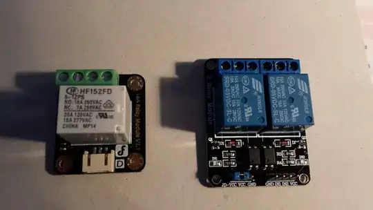
See linked thread that has a picture of the modules in question: need info about dc-dc boost converter
After blowing up a few modules, I dismantled them to understand their main components and principle design. The best one I had was using FDH055N15A MOSFET as the switch. The module linked above is using HY3912W MOSFET as the switch, both of which I have been getting reasonably good results of about 95% efficiency with during my experiments only I don't have any left now as I have blown all I had to hand by overheating them.
I started experimenting with other MOSFETs like IXTQ76N25T and FQP30N06L simply because I had some to hand, but my results were not great; I was getting more like 60% efficiency and struggling to output more than a few amperes.
I read a lot about Rds(on) value of the MOSFET and the lower the value the better, but I'm not sure how relevant it is and how big a deal or what effects it would be if it were to high or even what to high actually is. The two MOSFETs that have given good results have had about 6 mΩ Rds(on), I have also had reasonable results a FQP30N06L with 35 mΩ so I don't really understand why some MOSFETs don't want to play ball.
At the moment I have a TIP122 Darlington NPN transistor in my circuit and I am struggling to get any kind of usable current output.
Current setup with the TIP122 NPN is actually outputting to a 14 cell Nissan Leaf battery next to me that is 57.4V not 86.4V charge but the theory should be the same.
I have 0.503 A input at 12 V, 0.054 A output at 52.89 V, 6 W in, 2.85 W out, so about 47 % efficiency.
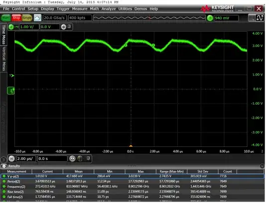
This scope probe shows the top scope connected to the transistor base gate, and the bottom probe connected between the inductor output and the diode, so the rising edge of the top scope is the signal from an ATmega328P turning on the transistor, at the same time the output pulls ground.
The gate is high for around 60 microseconds. As it falls low there is a big positive spike on the output. That is the charge from the inductor, right?
During the time the spike is high (above 52.89 V) current flows out to the battery as charge.
As the inductor runs out of energy the voltage falls back to ground rapidly and seems to stay at ground for a period of time before jumping back up to VIN. I wonder if this has to do with inductance. I don't know much about and would appreciate some explanations as to the patterns I see.
There is a large period of time that the transistor is off, leaving the output signal at 12 V, before the next spike as the transistor turns back on. If I shorten this time period trying to obtain more current throughput, I end up losing efficiency. Is there any explanation available as to what is happening? On the scope probe there is not much happening but in reality there must be something to do with inductance otherwise there should not be any efficiency drop for making use of that time.
Finally a picture of the actual circuit:
Any theory as to what I am not doing correct would be appreciated. I don't know much about inductance.
Edit:
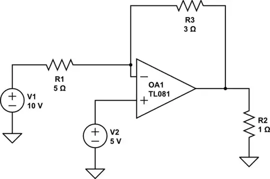
Schematic diagram of current circuit:
I have changed the inductor for a smaller one and I am now getting far better results. This is the new scope shot that is achieving 95% efficiency 100W 55V to 86V.
The diode I am using is a "Plastic Encapsulated Silicon Rectifier Diodes 1KV 10A" type 10A10.
Current testing measurements are as follows, ICR1=TOP and maxPWM is the PWM duty between 0-255 running from an ATMEGA328 clocked at 8 MHz.


