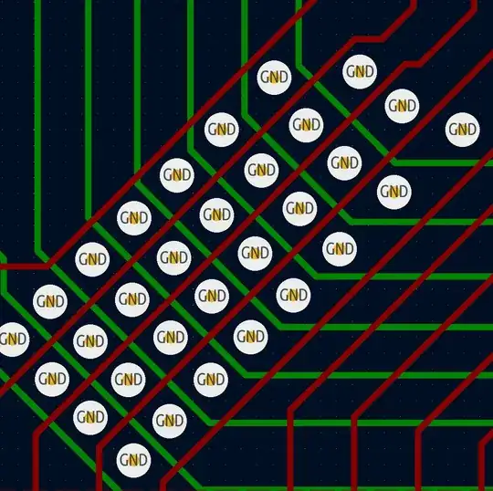
Your intuition is on the right track!
This should give excellent signal quality, but it is of course rather intensive on via usage. It would be nice to use fewer. If you need absolute best signal quality, maybe this would be the way to go -- but a 4-layer board would be less effort (unless perhaps you have special reasons those are unavailable). So you'll never see this in practice.
You can worsen it, incrementally, by pairing up traces into buses. Or triple or more, etc. This reduces the matrix significantly (via count goes as N*M for N top and M bottom traces crossing), and is still more than adequate for, say, LVCMOS signal levels (i.e., most MCUs, etc.), where the risetime is a few ns, corresponding to a wavelength of fractional meters. So, very little voltage will be dropped along a trace at any given instant, over these kinds of distances -- including the image (ground-return) currents that may have to divert around the edges of the slots created in GND by the other traces. (Which is a major part of where EMI and crosstalk come from in such areas.)
Also consider how much crosstalk is permissible. Digital logic input thresholds are typically 30-70% of VDD, and output drivers are very close to 0/100%, leaving a 30% noise margin. Parallel routed microstrip, at typical PCB tolerances, tops out around 10 or 15% coupling between traces, and at that, only for frequencies near the length of the coupling; i.e. if traces are paired along for 10cm length, then on the order of c/40cm or near a GHz, will have that degree of coupling. It will be asymptotically (i.e. 20dB/dec.) less at lower frequencies.
So there's really very little risk for routing parallel buses, and anywhere you can afford a GND "shield" trace inbetween, that goes down considerably -- or even just plain old distance, since the field drops off quickly beside a microstrip trace (on the order of (substrate thickness)/(edge-to-edge distance)).
Conversely, anywhere you need extra signal quality, precision, bandwidth, etc. -- consider a cleaner layout, or 4-layer, etc.
For reference, a few years ago I built this display adapter. See the links below to my website. It uses an Epson S1D13517 with support components (SDRAM and a serdes) for a parallel MCU interface to an LVDS LCD panel. It's built on 2 layers, and as you can see, there was some... congestion, in areas.
Transparent layers: https://www.seventransistorlabs.com/Images/DisplayCtrl_SDRAM_TopBottom.png
Top: https://www.seventransistorlabs.com/Images/DisplayCtrl_SDRAM_Top.png
Bottom: https://www.seventransistorlabs.com/Images/DisplayCtrl_SDRAM_Bottom.png
The top row of pins on the SDRAM (bottom chip) gets in the way of the traces reaching the far end; and there are a few VDD crossings in there (especially the one trace snaking along inside the top row of pins; note the bypass caps connecting along it).
The particular efforts I attempted here, are: making sure some ground pours between the bottom-side jumpers (up and down, crossing under the SDRAM top pin row); and allowing GND to stitch where traces/buses had to cross: in particular SDCLK, the longer trace down the middle; and VDD going to the graphics controller, off the top-right corner of the SDRAM, skipping 6 traces, layer swap, then 6 more traces.
Now, I don't have EMI results for this board unfortunately -- it was just a proto -- but if nothing else, I can confirm it is functional.

