I've designed a PIN diode RF switch driver, specifically to drive HP33000 series switches. Unfortunately, these are very old, and not much documentation exists, so I'd like to ask for advice from those more experienced with using these devices, as well as for general design tips.
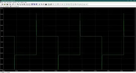
Looking through old HP documents(https://hpmemoryproject.org/an/pdf/an_58.pdf, https://www.hpl.hp.com/hpjournal/pdfs/IssuePDFs/1964-11.pdf), it is clear that switching time is improved by adding 'spikes' (see picture below) to the input waveform, to help overcome parasitic capacitances.

Unfortunately, I can't find any concrete details on what height or time scale these spikes should take place over. Are there typical rule-of-thumb values that I could start from?
Below is my design. I intend to take a TTL input on Vin, which is then used to drive the two MOSFETs. M1 has a low-pass filter, which is designed to be added to the +/- 5V output from M2, to create the characteristic spiking output. The spike height is adjusted using R6 / R7. The OFFSET input offsets the on and off state current draw based on an input voltage, and the current change between on and off is controlled by R9. The U2, U3, U5 bit at the end is a current source from an analog devices application note (https://www.analog.com/en/analog-dialogue/articles/a-large-current-source-with-high-accuracy-and-fast-settling.html). This is necessary because the PIN diode switches are current controlled. I use R15 as a dummy load to simulate the PIN diode switch input, although I suspect its behavior to be much more complicated.


