1

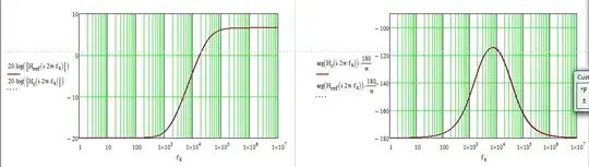
I'm reading AoE, there is a figure (p.26) for RC differentiator output and input voltages for step 5V input voltage with different slew rates (\$dV_{in}/dt\$). (It's time domain part. Only the rising edge of a step is shown.)

I understand the mathematics behind the chapter. So that \$V_{out} \approx RC\frac{dV_{in}}{dt}\$. But I'm trying to comprehend it in a physical sense, to carry out a mental experiment how electrons are "really flowing" inside the circuit and what's going on.

Many articles (when talking about step inputs) inspect the case when the input voltage is already 5V and a capacitor starts charging exponentially: \$V_{out} = V_f(1 - e^{-t/RC})\$.

But on the figure the input voltage is rising at a constant rate (e.g. \$dV_{in}/dt = 0.25V/ns\$). I imagine that at time zero the capacitor acts like a short circuit, so that all voltage "goes" to the resistor. Which "generates" \$I_R = I_C = I = \frac{V_{out}}{R}\$. This current charges the capacitor \$I = C\frac{dV_c}{dt}\$, so that voltage across the capacitor changes (increases).

At the beginning I believe that the input voltage change is greater than the capacitor voltage change (\$dV_{in} > dV_c\$), so that \$V_{out}\$ increases. At the same time as the output voltage increases, the current also should increase, which increases the capacitor rate of charge (\$dV_c/dt\$). The capacitor should be charging as \$x^2\$ (because the current is not constant). At some point in time the difference between \$dV_{in}\$ and \$dV_{c}\$ starts to decrease until it becomes zero. After that increase of \$V_{in}\$ equals to the increase of \$V_c\$ and \$V_{out}\$ stays const. (I could imagine it as pulling a spring at one end, the spring stretches and after while the other end of the spring jumps towards the first one)

I've found several answers on this topic but can't get the answer consistent with my thoughts:

If we calculate the output voltage amplitude, we get: $$ RC = 50\Omega * 10^{-12}F = 50 * 10^{-3}ns = 0.05ns $$ $$ V_{out} = RC\frac{dV_{in}}{dt} = 50\Omega * 10^{-12}F * 0.25 * 10^9 V/s = 12.5mV $$

Which is consistent with the figure. But using the formula from the first answer and plotting a graph, it seems it gives a different answer. $$ V_{out}=V_{in}e^{-\frac{t}{RC}} $$ Where: $$ V_{in} = \frac{dV}{dt}*t $$

Powers of 10 are changed. But max value is different (4.6 vs 12.5) and the waveform is different.

According to the second answer we get that the current through the capacitor (if all the input voltage change was only across the capacitor) should be: $$ I = 10^{-12}F * 0.25 * 10^9 V/s = 250 \mu A $$

Which gives us (UPD 06.07.2022): $$ V_{out} = IR = 250 * 10^{-6}A * 50\Omega = 12500 * 10^{-6} V = 12.5 \mu V $$

At this level should be the voltage across the resistor (which is also the output voltage) to "generate" the current which charges the capacitor at the same rate as the input voltage increases. (P.S. The original post contained an error V=I/R, fixed this issue).

My questions are:

  • What is the capacitor voltage waveform? (Is it S-like?)
  • How to calculate the difference between \$dV_{in}\$ and \$dV_c\$ because of which \$V_{out}\$ increases?
  • Why do the answers from the linked topics give different results?
valeroso
  • 11
  • 2

2 Answers2

3

The picture in the OP question is a little "biased".
Don't forget that it was taken with a scope with "bandwidth" limited.

Here is a simulation with one bandwidth in mind.
Vs is now more representative of the OP picture.

enter image description here

Here is a Maple sheet to confirm levels of outputs (at 0.25V/ns).

enter image description here

enter image description here

enter image description here

Antonio51
  • 11,004
  • 1
  • 7
  • 20
  • thank you for your answer. Am I right that the bottom graph V(vs)(V) is the voltage waveform for the \$C2\$ capacitor, but \$C1\$ waveform would be the same? Is the part of the circuit in the purple box is a "utility" to make input voltage is we wanted (with a slope)? – valeroso Jul 06 '22 at 14:44
  • If we divide the output voltage by the input voltage slew rate (\$V_{out}/\frac{dV_{in}}{dt})\$, we'll get \$12.5mV/0.25V/ns=0.05ns\$, as much it takes to get voltage across resistor. But on the OP graph it takes almost 4ns to get \$12.5mV\$ output voltage (which is almost 100 times more). Is this because of the capacitor, does it steal voltage difference? How to calculate the steal-rate? Why 4ns, not 10, not 1? – valeroso Jul 06 '22 at 15:31
  • Vs is in fact the same as Vo ... but "corrected" with the limited bandwidth (don't care what is in the box, 120 MHz low-pass). – Antonio51 Jul 16 '22 at 09:22
0

You are doing well to analyze this but let me add some key points: (rather than explore the assumptions in the links)

  1. The voltage across a capacitor remains exponential with a step voltage in my examples because the breakpoints are far apart by 10x.
  2. The RC=T(63%) step response of the resistor/capacitor if slower than the input slope will always lag the input. If faster then it is closer to following it.
  3. The initial condition must always be included in calculations.
  4. I made a simulation for you to show the response of simple RC low pass cascaded with high pass. I am hoping this picture is worth 2k bytes. ;) It plots Voltage and below it Current in yellow for the input, and 2 other components. LPF=> HPF with the same resistance at source and load. You can change any variable there and simulate any ideal part or add series resistance and inductance to make it real as all passive parts have some values of RLC.
  5. The first cap C1 reaches 63% (1-1/e) of 5V in 0.5ns
  6. This low pass filter (LPF) can be correlated to a half-power (-3dB) frequency response using \$RC=T=1/\omega_o\$.

100MHz pulse 10% d.f. = 1ns pulse
R1C1= 0.5ns so the 63% of 5V is 3.15V shown on Cap voltage Max. enter image description here

Additional RC load can be added by pressing the switch. This reduces the rate of change further with more lag and lower peak voltage.

This may simulate your Vin. Then I added an HPF RC filter with the switch to show the effects.

enter image description here Because the Vout is C coupled the average DC voltage must return to 0V.

Tony Stewart EE75
  • 1
  • 3
  • 54
  • 182
  • Thank you for your answer and the online tool. Am I right, that you're using low-pass filter on the left as an integrator to get a slope voltage for the high-pass filter on the right? It's weird for me right now, that online tools doesn't give step voltage source element with configurable slope. – valeroso Jul 06 '22 at 14:39
  • Is it correct that input voltage slope (\$dV_{in}/dt\$) multiplied by capacitor capacitance defines maximum current which would be in the circuit (going through the capacitor)? – valeroso Jul 06 '22 at 14:39
  • Yes. Slew rates must be defined by some added method. By RC and buffer or just RC or by current limiter to simulate real source so Z source Z(f) must be known then estimated then modelled. Or simply add low R big C. The plot in AoE was possibly an active current limiter – Tony Stewart EE75 Jul 06 '22 at 14:48