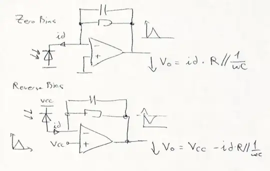
When I see TIA schematics, I can see either the photodiode to GND or against VCC. What is the difference?
Asked
Active
Viewed 631 times
3
-
1Both of your circuits produce zero bias across the photodiode. If you want reverse bias in the second diagram, set the non-inverting input to GND, and deal with the fact that the output voltage will be below ground. – The Photon Jul 02 '22 at 13:08
-
1Or use the first diagram, but apply a negative voltage to the PD anode. – The Photon Jul 02 '22 at 13:09
1 Answers
4
First: photodiode is a current source, which suggests its internal resistance is mighty high...often hundreds of Megohms for a small-area diode.
Zero-bias (GND):
- minimum leakage current and temperature-induced currents added to photo-current
- minimum noise
- highest capacitance, slowing response time.
High-reverse-bias voltage source (Vcc):
- less diode capacitance, for fast response time.
- leakage current is higher, causing DC offset.
In some circuits, the photodiode is placed between op-amp "-" and "+" inputs - this is equivalent to zero-bias operation.
glen_geek
- 23,591
- 1
- 22
- 50
-
Also it seems the high-reverse-bias, would need a Vref on V-, not on the other case right? – nowox Jul 02 '22 at 11:58
-
1
-
1Any bias supply *must* reverse-bias the diode. The resulting leakage currents are in the same direction as photo-current. So if anode attaches to bias-supply, the supply must be more negative - a cathode attached to bias-supply would require V+. – glen_geek Jul 02 '22 at 12:47
-
1Reverse bias also widens the depletion zone, which improves the quantum efficiency, especially in the infrared. – John Doty Jul 02 '22 at 19:46
