Expanding on Andy's answer: note that analysis of this circuit, in general is kind of dubious. Let me explain in what sense I mean that:
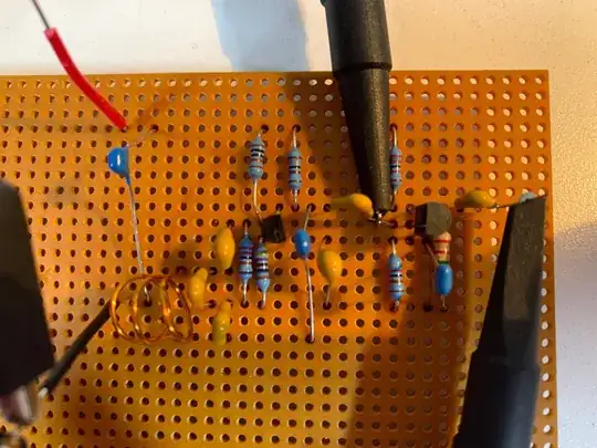
Consider the inductance between most any two points in the circuit. The veroboard layout and THT components give paths of several cm in length. The inductance of free space is \$\mu_0 \approx 1.257 \mu \textrm{H/m}\$. So these lengths correspond to some 10s of nH, give or take a geometric factor due to their cross section and relative placement (i.e.: wide loops of thin conductors, have higher inductance than thin loops of wide conductors). Corresponding to some 5's of ohms at 82MHz. Maybe not a lot versus the ~kohm circuit impedances, but keep in mind these inductances are coupled as well, so where some 10s of mV drop across one, a few mV also appear along neighboring traces. There is no concept of ground in such a circuit, not as we would like to consider it -- everything is floating somewhat relative to everything else, a little bit squishy rather than the hard and solid connections we would like to think we have.
Likewise, your scope probes have considerable effect on the circuit. A typical 10x probe is on the order of (10pF + 500R) || 10M. That is, at DC it looks like 10M, but at very high frequency it's closer to 500 ohms (or maybe low kohms, depends), and inbetween, the equivalent capacitance and resistance is also somewhere inbetween.
So it all looks rather messy. We could run a simulation of the schematic as given, but we're almost certain to get significant differences in waveforms (amplitude, frequency) -- even if accounting for probe impedances. It's not exactly that such a circuit is hopeless -- but it's a lot harder to work with, than it might look at first.
So the first challenge is just seeing how the system (when built this way) is more complicated than the schematic suggests. The second is finding ways around that.
What should we do to solve this?
Use RF design techniques.
First, build everything on ground plane.
You can get veroboard or pad-per-hole or whatever perf you like, with plane (mesh really, since, it's perforated with holes, but it's still better than nothing), and that helps a lot. The wide area conductor forces currents to flow on one side, near the conductors routed over it -- reducing stray inductance, and greatly reducing coupling between traces. This is the first critical step to being able to easily analyze circuits: we can again mostly ignore the coupling between traces.
With a ground plane, we can measure a voltage difference at a point (with respect to a point on that ground plane -- notice we need to maintain good shielding when we make such a measurement -- say by soldering a coax shield directly to the plane), and be reasonably confident that what we measure is what's really going on in circuit, and not an artifact of strays or probing technique.
Second, use lower impedances.
More generally: appreciate that impedances are lower by necessity, and work with that.
In fact, impedances ultimately are proportional to the impedance of free space, Zo ~ 377 ohms. Transmission lines are typically lower than this (again, due to geometry factors -- hence coax being 50/75 ohms, twisted pair 50-150, twin lead 200-600, etc.) There is no such thing as 10kohm transmission line, so we can leave such impedances aside, at least for signal purposes! Now, we can have circuit impedances significantly different from these, either when the transmission line is very short (~cm is still quite short relative to the ~3m wavelength of this frequency, or even the wavelength of most harmonics thereof), or when it's resonating (basically, reflections pile up N times, giving something on the order of Zo*N or Zo/N).
Mind, we don't need to consider transmission lines in a compact circuit like this, we can use their equivalent inductance and capacitance (low frequency / fractional wave approximation) -- but we still must use them if we connect to anything at some distance, i.e. by cable, probe, antenna, etc. (Indeed, the probe loss can be seen as the fact that power flow is required to sense the signal; it can be made arbitrarily small with clever probe design (especially active types), but cannot be made zero.) And since reflections would be a problem, we prefer to use terminated transmission lines, even if we don't need the available signal power, or the low impedance, at the far end (say, where it's going into an oscilloscope's input buffer circuit).
So, for the oscillator itself, I mean, it's running, clearly it's not having too bad of a time. The signal at its collector is probably much less than it could be, with the 1.8k supplying it, but that's not even a big deal, since your JFET will have voltage gain, and a lowish input voltage is probably a good thing overall. (The other way to get a low voltage, of course, would be making the resistance very low, maybe 100 ohms or less. Which might be an excellent idea for coupling directly to a coax cable, for example -- say if the buffer had to be at some distance, for some reason.)
As for the buffer, we have several things to consider:
- Input capacitance: what effect does this have on the oscillator (loading)?
- Output power (or voltage, or gain): is biasing adequate (smaller drain resistor, or change to an inductor)? Is it well matched to the load? What is the load? (Again, a scope probe is quite a strong load compared to the schematic as shown!)
- Feedback: a common-source amplifier exhibits Miller effect, i.e. Cdg is multiplied by voltage gain, which means effectively the input capacitance depends on voltage gain. And output voltage depends on load, so by chain, there will be some sensitivity of the oscillator on the buffer load. Which means it's not really a great "buffer", is it? Now, 2N3819 is a pretty small JFET (low capacitances, modest Rds(on)), so this might not be much effect, but then again if you're looking for a quite stable frequency, maybe this bears more consideration.
The usual way to avoid the last one, is a common-gate or cascode circuit (the latter of course incorporates the former). The source input side has a fairly low impedance (~1/gm), which is a good match to transmission lines (hence a common input circuit for radios) but might not be so desirable here; the drain output is well isolated (Cds is small) so it serves well as a buffer. Noninverting diff pair is also a good candidate: the input side looks like a source follower, thus having mostly Cgd (with no Miller effect), causing little load on the signal source; the output has current and voltage gain.
To say nothing of matching, of course; it could be that you can increase your output power by using a capacitor divider from the oscillator to the JFET, for example, or some manner of LC network; or a matching network or transformer at the output (so the impedance seen by the drain can be fairly high, getting a reasonable voltage swing thus using most of the power available from the transistor), to match to a low impedance load (preferably using coax straight into the scope at this point -- probes aren't great at this frequency), but that's a much more complex (ha) topic to cover in another answer...
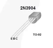
Finally, the scope -- the DS1054Z is only 100MHz or so; you're lucky to see any bounce/flattening of that waveform at all! Likely, the real waveform is crunchier than you can see here, but you can only guess at what that might look like. (On the upside: 2N3904 doesn't really go fast enough to do anything crazy, and probably it's some flattening due to saturation, and a bit of ringing due to slamming into saturation every cycle. 2N3819 can oscillate at a bit higher frequencies (>400MHz), but you'd have to be pretty unlucky with layout I think to excite that.)
If you can get a one of those cheap handheld spectrum analyzers, you can get a better idea what's going on with the waveform, by looking at the higher harmonics.
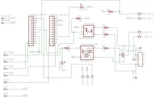 (nb. corrected diagram adding ground between series 68 pFcaps and corrected Vout)
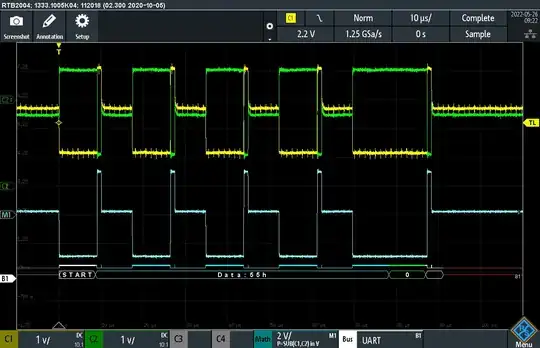
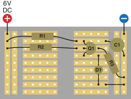 As expected, there was a noticable small increase in frequency and amplitude when the scope probe was removed, but not by as much as I feared.
Then I looked at the harmonics up to 350 MHz. The photo speaks for itself
