1

I have the below configuration for driving a half bridge converter:

half bridge configuration

As you can see I use just one signal to turn off and turn on low side and high side MOSFETs. I putin a delay while turning MOSFETs on to avoid short-circuit in the half bridge while I turn them off as fast as possible. As you can see in following pictures output voltage and gate source voltages in MOSFETs are all correct.

output voltage

gate source voltages

I have still current spikes that cause a lot of energy loss in my circuit:

current spikes

What are these spikes and which element making them? I guess it's because of drain-source parasitic capacitors but I'm not sure about it. On the other hand the higher frequency causes more energy losses so I can't use my MOSFETs in higher frequencies.

EDITED: To ensure this problem is not related to what is called shoot-through I made a modification to my first design as below:

modfication

v1 has 56% duty cycle and v2 has 50% duty cycle with 3us delay so gate signals of both transistors are as follows:

signals

The blue signal is related to high side transistor and pink one related to low side. Now I'm sure both transistors have dead-time and each of them will turn on when other one absolutely is in off state, but we still have spikes as follows:
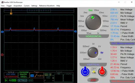
spikes

JRE
  • 67,678
  • 8
  • 104
  • 179
H.hashemi
  • 19
  • 3
  • i did mistake in gate source resistors but problem exist any way.i should replace 1kohm resitors with 2kohm resistors so gate source voltage became 10 volts instead of 20volts – H.hashemi May 30 '22 at 15:54
  • Your 2 kohm pull up/down resistors won’t cut it. Also, 1 kohm gate resistors is way too high. Try 10 ohm. Have you considered a dedicated MOSFET driver, or two? – winny May 30 '22 at 15:54
  • i just exame it with 10ohm resistors and i got worse response.I mean worse spikes with longer amplitude.note there is no interfereance between mosfets while i turn them on or off i'm sure about it so problem don't originated from gate resistor value – H.hashemi May 30 '22 at 16:00
  • That’s because your turn off is too slow (root cause) and you are trying to rectify it with slower turn on. You have several problems at once and you can’t fix it with a single component value change. – winny May 30 '22 at 19:21
  • You’re probing the driving voltage sources whereas you should be probing Vgs for each MOSFET. You have shoot-though for sure. – winny May 30 '22 at 19:24
  • 1
    Generally speaking, you need a gate driver for this application - it's rather hard to drive those gates otherwise, if you care about minimizing switching losses. – Kuba hasn't forgotten Monica May 31 '22 at 19:29
  • _”Now I'm sure both transistors have dead-time”_ Show it. – winny Jun 01 '22 at 11:40

2 Answers2

4

The question has been modified but, before the modification, the shoot-through current was peaking at about 5 amps and, after adding anti-shoot-through circuits, that peak is down to 1.2 amps as far as I can tell. That sounds like a definite improvement and, the remaining current could easily be MOSFET capacitance (a common enough problem).

$$\color{red}{\boxed{\text{Answer to the OP's original question}}}$$

Think about your circuit: -

enter image description here

So, every time V1 changes state there will be a current pulse passing from Vcc to GND because both MOSFETs will be partially fully on for a short moment in time. This is called "shoot-through" and you need an "anti-shoot-through" circuit. This can be made from logic gates and RC delays or you can use a Proper half-bridge driver IC that has this feature built in.

Logic gate version from this answer: -

enter image description here

But I put delay while turning MOSFETs on to avoid short-circuit in half bridge while I turn them off as fast as possible.

That would not work - you need "dead-time" where both MOSFETs are unambiguously "off".

Andy aka
  • 434,556
  • 28
  • 351
  • 777
  • I am 100 percent sure these spikes is not related to what you call it as `shoot-through` .to proof it i just make modification on my first desgin so i'm 100 sure there is `dead-time` between transistors which both of them are off but current spikes are still exsited – H.hashemi May 30 '22 at 16:48
  • i did edit my question to make sure problem is not related to `shoot-through` – H.hashemi May 30 '22 at 17:26
  • 1
    @H.hashemi Once an answer appears, you should not modify your question without agreement because, if it invalidates those answers it causes more work. – Andy aka May 30 '22 at 17:33
  • 1
    You were getting 5 amp peaks before and now, with the modification (as per my suggestion), you are getting peaks of about 1.2 amps. Do you not see that improvement? – Andy aka May 30 '22 at 17:36
  • neither 5amps nor 1.2 amps is not solution.because (in practical on high frequencies more than 1khz) this circuit will draw huge current from power supply and transistors will got too hot – H.hashemi May 30 '22 at 17:46
  • Have you calculated the power dissipation? Why not compute it in your simulator. – Andy aka May 30 '22 at 17:53
  • in simulation mean of power dissipation converge to around zero. i think it's because of negative current peaks that retrive power to battery.so i will consider adding capacitor in parallel to my power supply since power supply can not absorb power.so If I understood correctly we should not care to this current peaks – H.hashemi May 30 '22 at 18:40
  • 2
    Maybe - but make sure you have it simulated correctly before making final conclusions @H.hashemi – Andy aka May 30 '22 at 18:43
1

This is an alternative to your circuit. Use of Zener 20 V.

enter image description here

To show the "internal" current, I have checked this @ 1 MHz. (0 nH < Lind < 20 nH, step 5 nH).
Lind=10n remove "over-current" (red curve, measured at power supply).

enter image description here

And here for a "lighter" load.
NB: the problem is that the two MOSFETs are not really "complementary" about specs.
Lind=10 nH do "well" its "job".

enter image description here

Antonio51
  • 11,004
  • 1
  • 7
  • 20
  • your answer was amazing thank you in advance.but it made some questions for me.1-does it work in lower frequencies like 1Hz since i want this circuit to be varibale frequency inverter.2-Does it have formula to calculate "RL" branch which you added to the source of MOSFETs?3.did you ever calcualted power dissipation in this `RL` branch as i know adding any element to this path cause extra power dissipation in circuit.4-what is the purpose of R1 and R2 resistors?5can you explain more about you circuit fundamental especially about C1 D3 D4 as i know D3 and D4 should be used when load is inductive – H.hashemi Jun 01 '22 at 16:08
  • Be aware that simulation is done in the case of 2 resistors' "big" loads (R7-R8-C1 for DC midpoint). Q1-yes, it does. I used high frequency to check if it does work at that high frequency and "how". Q2- no formula, just limiting di/dt, and interactive use of the simulator. Q3-not calculated, but very low because R shorted by L low, could check, ok. Q4- R1 & R2 just used to measure current in that branch X1 and X2 (MOSFET Id currents). Q5- yes, right. D3 & D4 just in case if the load was inductive. C1 is used if the bridge is complete (here, pseudo-bridge). – Antonio51 Jun 01 '22 at 16:40