1

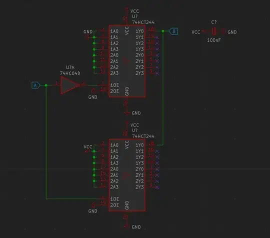
Say I have two driver gates hooked up to each other in the following arrangement:

enter image description here

In theory when A goes low, for a brief amount of time B will be shorted while the 7404 inverter gate switches. Around seven nanoseconds at VCC = 5V according to the Nexperia datasheets.

a) How worried should I be about this in general, does this cause problems at higher frequencies (5 MHz for example)? What if this period is longer, say 20 or 50ns?

b) If this is an issue, how is it usually handled? Do I place buffer gates to try best match the propagation delays? Or should I place resistors at all outputs of every driver gate in my schematic?

Thanks in advance!

Edit (2023-02-18): For future reference, there is a section about shorting outputs in the 74HC(T) user guide:The life of the IC will not be shortened if not more than one
input or output at a time is forced to GND or VCC during
in-circuit logic testing (“back drive”) as long as the following
rules are obeyed:
• maximum duration : 1 ms
• maximum duty factor : 10 %
• maximum VCC : 6 V

Zsigu
  • 13
  • 4
  • 2
    Brief shoot-through is sometimes more tolerated in logic than power circuits where power levels are much higher. You could throw in small series resistors and that would nip the problem. – DKNguyen May 21 '22 at 16:18
  • You have to also take into account that the 74HC04 inverter will also delay the output, so the output enables are not driven with an ideal out of phase signal to begin with. And I get this is a hypothetical question, so you are looking for solutions to some problem X by asking about solving it with Y. But why not simply use one HCT244 and just control all input data pins with the signal? – Justme May 21 '22 at 17:22
  • This isn't a well contrived situation: why not simply wire A to 1A0 and be done with it? You aren't gaining anything by wiring two inversely in parallel. – Tim Williams May 21 '22 at 20:20
  • @TimWilliams - I'm presuming that this is a simplified example, and it's actually essentially double-buffering between two sets of output signals. That being said, I'm not the OP. – TLW May 21 '22 at 20:43
  • 1
    @TimWilliams This circuit achieves no real purpose; what I have in practice is more akin to a PCI bus, where different components output to a common 8 bit bus when their address is selected. The issue is the same, that sometimes the next driver gate turns on one or two gates worth of time ahead of the previous one turning off. – Zsigu May 21 '22 at 21:22
  • @Zsigu - I might suggest that you pick a target impedance and design the entire bus to said impedance. Matching drive strength / bus / termination impedance will reduce ringing and likely will mitigate shoot-through as well. Your drive chip works out to ~140 ohm min output impedance to not exceed absolute max, which is about right for 10mil surface microstrip (https://www.pcbway.com/pcb_prototype/impedance_calculator.html). This would still be stressing the chip somewhat. – TLW May 21 '22 at 21:48

2 Answers2

2

a) How worried should I be about this in general, does this cause problems at higher frequencies (5 MHz for example)? What if this period is longer, say 20 or 50ns?

As always, it depends. Some things to watch out for:

  1. Thermal issues. You're drawing a burst of current during the transition, which can overheat components.
  2. Gross overload failures. Output impedance is too high for many logic circuits to really cause this sort of failure - but can be a problem in some cases.
  3. Power supply droops. Again, you're drawing a burst of current during the transition. If you don't have proper decoupling (not just 'how much' but also 'how much impedance' and 'how well-placed are said capacitors'), this can cause problems.
  4. Interference. Transient shorts can cause 'amusements' with RF noise, as well as general power supply noise being coupled into other components.
  5. Current draw. More of a problem with batteries, but still worth noting.
  6. Longer-term failures due to e.g. electromigration. More of an issue with e.g. digital IO of microcontrollers than it is simple logic chips, but can still be a concern.

Shorter bus contention is generally - not always - less of an issue than longer bus contention. Among other things, there is always a certain amount of inductance present, which helps limit max current for a bit.

In this case:

Absolute maximum output current is given as 35mA. I'd be concerned about this. Especially given this chip has a specified minimum input rise/fall rate (indicating that internal output shoot-through is likely a potential problem - which doesn't bode well for external shoot-through either) (annoyingly, this is specified as a maximum time/input voltage change.), and doesn't specify an output voltage-versus-current curve beyond 6mA.

Personally? I wouldn't use this design unless either:

  1. Failures aren't a big deal, including failure modes like "the chip shorts VCC to an input signal" and "the chip catches fire" (The latter is unlikely! But not impossible.) (What is the chip driving? Are there potential problems if the output signal ends up floating for an extended period at a forbidden logic level? Etc.)
  2. I added enough resistance to the output to limit current to below spec'd ratings even when shorted.
  3. I measured and made sure that the transient wasn't hitting above spec'd limits on the actual specific parts being used. (Fine for a one-off, not so fine if I'm making a hundred units.)
  4. I got something from the manufacturer saying it's fine. (It may be worth asking! Worse comes to worse they ignore you.)
  5. I was using a part that specified an output voltage-versus-current curve all the way to half VCC (and the resulting values were within spec).
  6. I adopted something like the below:

b) If this is an issue, how is it usually handled? Do I place buffer gates to try best match the propagation delays? Or should I place resistors at all outputs of every driver gate in my schematic?

If this is an issue, one approach may be a break-before-make design:
schematic

simulate this circuit – Schematic created using CircuitLab

(Adjust numbers as appropriate.)

(Given that your OEs are inverted, you probably want to swap this around to a make-before-break with an OR and NAND. Basic idea is to ensure that you never have both enabled at once.)

Be aware that both gates here should be schmitt-type. Be aware that this will result in the outputs potentially floating for a moment.

(Depending on what said signal is being driven with, you may be able to simply drive the two inputs from e.g. two IO pins instead. Do take care with this approach, as it now means something misdriving the OE signals can cause hardware failure.)
TLW
  • 608
  • 4
  • 9
  • 1
    I'll look into how and if I can use a break-before-make design for a lot of components without using up too much pcb space. Thank you so much for the thorough answer! – Zsigu May 21 '22 at 21:45
  • (There's also a similar circuit with two cross-coupled NOR or NAND gates, although said circuit is more difficult to tune the delay of.) – TLW May 21 '22 at 22:19
1

It's called bus contention. TI's appnote SDYA009C (1997) "Designing with logic" goes in depth to calculating the relevant parameters.

To quote them:

If several bus drivers with 3-state outputs are connected to a single bus, it often cannot be ensured that during the time when switching from one bus driver to another, both are not simultaneously active for a short time. For this short time, a short circuit of the outputs exists, resulting in an overload of the circuit. This situation is known as bus contention.

Short bus contention, with a duration of a few, or of a few tens of nanoseconds, causes a temperature increase of the component in question of about 10°C. Therefore, a degradation of the reliability of the component is unlikely.
Furthermore, in well-designed systems, the period of bus contention is high compared to the duration of a single instance of bus contention (period:duration > 10:1).

They also mention the possibility of it happening in power-up state, and I know from experience that one cab fry your chips.

Jeroen3
  • 21,976
  • 36
  • 73
  • 1
    Assigning an arbitrary temp rise to such an incomplete situation is... well, appnotes in a nutshell, go figure. – Tim Williams May 21 '22 at 20:19
  • My usual worry would be electromigration issues, not so much temperature changes... though this is mainly an issue with VLSI. – TLW May 21 '22 at 20:43
  • 1
    @TLW - Don't be so fast to discount electromigration issues. VLSI or not, if you can't determine what the current is during the shoot through, or overlap condition, and don't know how often this condition is going to occur (once every 100 ns is a lot different that once at turn on), it's probably not possible to say that electromigration is not a concern. – SteveSh May 21 '22 at 21:16
  • 2
    The current pulses can also be a source of EMI, which will be of concern in some applications. Source (series) termination of each driver (to match the bus impedance) can also serve to limit the magnitude of the contention current. Better to eliminate the contention to begin with. [Cross-coupled NAND or NOR gates](https://electronics.stackexchange.com/a/430379/11683) can be used to insure that the enable signals never overlap. – Dave Tweed May 21 '22 at 21:31