1

I just ordered a PCB that uses a certain battery holder. I am looking at the 2D footprint and 3d model now thinking there must be some error, but I wanted to confirm this before I recall the PCB, also I don't spot too many errors these days so I am skeptical of myself.

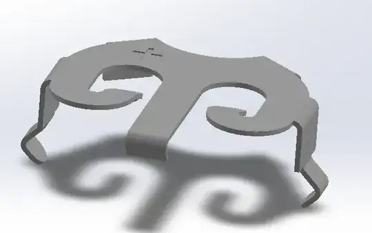
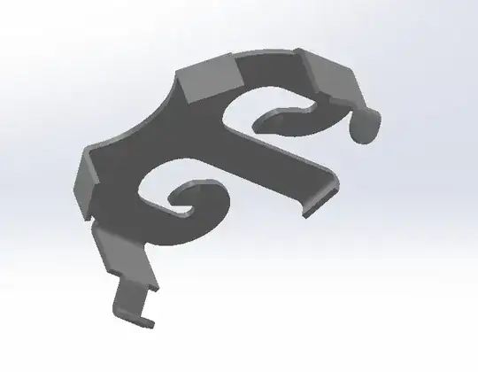
Looking at the schematics, pad 1 & 2 are specified to be + and - respectively. If we take a look at the 3d model in the STEP file and 3d pictures on the datasheet how is it possible that 1 and 2 are isolated? The frame is metal and these two pads are connected... Is MP1 meant to be the negative? datasheet
footprint

3d pic 2

3d pic 1

Feynman137
  • 1,223
  • 5
  • 24
  • Where did you get the symbol and footprint? I've found numerous errors with them when obtaining from manufacturer or a source like Ultra Librarian, GrabCad, etc. – JYelton May 06 '22 at 23:09
  • Mouser is where I got it, my experience with them has been good – Feynman137 May 06 '22 at 23:10
  • 1
    The 3D file also doesnt match the datasheet. 3D seems through hole, datasheet and land patterns seem to be for SMD. – Wesley Lee May 07 '22 at 00:26
  • I think you are right here, Keystone coin cell receiver# 2895 is THT and 2894 is SMD but they both have this labeling issue on Mouser. @WesleyLee – Feynman137 May 07 '22 at 00:29

1 Answers1

3

What you have there is a "coin cell retainer" not a "coin cell holder". The difference:

You need to make a PCB layout symbol for your part that includes two outer pads for the retainer plus a center pad for the PCB contact to the cell.

Reference also this question in stack exchange

*My site

Davide Andrea
  • 16,164
  • 4
  • 33
  • 62
  • I see now the difference between these two terms! But why would the 2d footprint label 1 and 2 as + and - when 1 and 2 are both positive and the center plane is negative? Also the reference is great – Feynman137 May 06 '22 at 23:29
  • 3
    A good question, whatever the answer is, the footprint doesn’t match the schematic part. 1and 2 are indeed both positive. – Frog May 07 '22 at 00:20