3

In this particular instance, I'm using a STWD100NYWY3F with a 3.3v Vcc and feeding it's !EN input from a 5v TTL signal (from a SN74LS00D). The absolute max input is Vcc + 0.3v. I propose to just put a 10 kΩ resistor between the source signal and this pin. I am operating under the presumption that there's a protection diode from the pin to Vcc and that the resistor will act as a current limit for that diode and the two together will act as an effect level shift.

Is this assumption sound? Is it a frequent practice? Or is it an awful idea?

nsayer
  • 1,543
  • 1
  • 18
  • 35
  • 1
    Depends on the input impedance of the load. It'll present as a resistance in series with your 10k and make a voltage divider. It could throw the voltages off if it's a low enough impedance. – Kyle B May 05 '22 at 20:13
  • Yes, it can be feasible. This depends on the RC delays you can tolerate. Normal drivers are in the 50-ohm range +/- 50% and input capacitance ought to be on the datasheet and trace capacitance can be estimated or calculated. – Tony Stewart EE75 May 05 '22 at 20:24
  • 2
    Using the internal ESD diodes as a clipper is not recommended. They are small and are designed to only conduct a few times in relation to the lifetime of the chip. – Aaron May 05 '22 at 20:53
  • Is it really TLL 74LS IC? then use 1K pullup and add Schottky diode to 3.3V and ensure power sequencing is controlled to protect CMOS. – Tony Stewart EE75 May 05 '22 at 21:11
  • @TonyStewartEE75 yes, if I was going to add a 2nd part, it would be a diode to make a diode+pullup shifter. The delay/speed here is not a concern - the EN pin signal is exceedingly slow - less than .01 Hz. – nsayer May 06 '22 at 03:53
  • called "a positive diode clamp" – Tony Stewart EE75 May 06 '22 at 05:53
  • 1
    Please can you edit your question and clarify the part number for the TTL source signal. – TonyM May 06 '22 at 11:14

5 Answers5

7

It's generally not a good idea to deliberately put significant current through protection diodes.

The current can have side effects like increasing power supply current and spilling out of nearby pins.

Two resistors solves the problem provided speed isn't an issue.

You would be exceeding the datasheet absolute maximum input voltage specification:

enter image description here

Can you get away with it? Probably. Should you? I don't think so.

Spehro Pefhany
  • 376,485
  • 21
  • 320
  • 842
  • 1
    Not to mention that not all devices use clamp diodes to the supply for ESD protection. Some have snapback structures, so really good to avoid trying to use the protection diodes as described by the OP unless the manufacturer specifically allows it. – John D May 05 '22 at 21:00
  • 1
    With a 10 kΩ series resistor, there wouldn't even be 500 µA if it was a dead short from 5v to ground or a low input to 5v. Is that a "significant" current to you? – nsayer May 06 '22 at 03:45
  • 1
    p.s. my last question was genuine - I fear the wording may have sounded snarky. – nsayer May 06 '22 at 03:59
  • Yes, it could be. I don't necessarily buy the electromigration but other issues such as raising the 3.3V supply and increasing Idd are possible. It's not enough current to cause latch-up type problems most likely even at elevated temperatures, but there are other possible problems. If it's a hobby circuit, maybe nothing to worry about. If you're shipping 10K units a month then the 0.001 penny for a resistor is good insurance. – Spehro Pefhany May 06 '22 at 04:19
5

No, not really feasible. And it is a terrible idea to actually utilize the input clamping diodes as a designed feature, rather than just allow them to clamp under fault or accidental conditions.

Besides it would leak current into 3.3V supply node, and if 3.3V is not present or there is not enough consumption, the clamping current will try to rise the 3.3V node from 0V to some undetermined voltage, or even beyond 3.3V.

And there are a lot of unknown factors. First of all, a 5V TTL output would never give out 5V, it might be only 4V, and with about 0.4mA current the voltage might be typically only 3.4V. And it does look like the watchdog has CMOS inputs, but that or protection diodes or maximum injection current through clamps is not mentioned.

Use of a voltage divider, but due to the TTL output, the output varies a lot with the load, and to be within specs, the divided down voltage needs to be between 2.31 and 3.3V. It might be worth to have a resistor to pull-up the TTL output high, and then a resistor divider to bring voltage down to 3.3V level.

Another option is to just use 5V for the watchdog, but you'll still need a pull-up resistor, to keep the voltage above the required 3.5V.

Justme
  • 127,425
  • 3
  • 97
  • 261
  • The problem that I'm trying to solve is that the WDI pin has a 3.3v logic input, and - though it has been working ok - the minimum high level of 0.7*Vcc is 3.5v, which is too high. – nsayer May 06 '22 at 03:48
  • I saw a super-cheap solar-powered garden light where the solar panel current all went through a clamp diode (/EN pin of a boost converter controller, turning off the power to the light, and charging the battery at the same time). Although perhaps the chip was designed for that. – user253751 May 06 '22 at 11:32
4

While what you are proposing is technically okay, from a schematic point of view, when considering the effects based on the actual parts in use, it's not a good idea. There are two issues to consider, thermal and electromigration. The ESD diodes and paths inside the chip are not usually documented such that you can reasonably design with them.

Electromigration

Even when the current does not cause thermal problems, the diode current could still create a reliability problem. There is a maximum lifetime current rating for any electrical signal path due to electromigration. The electromigration current limit for the diode current path is typically limited by thickness of the internal traces in series with the diodes. This information is not always published for amplifiers, but needs to be considered if the diodes are active for long portions of time, as opposed to transient events.

Source: Analog.com Using ESD Diodes as Voltage Clamps

Aaron
  • 7,274
  • 16
  • 30
  • Really good point about the electromigration issue. Some designers use the ESD clamp diodes to limit undershoot & overshoot on improperly terminated signals. This is not what they are there for. – SteveSh May 05 '22 at 21:56
  • ESD diodes are usually rated at 5 mA. They are tiny (low pF) to react faster than the FETs. This is a fallacy that electromigration is caused by low current. We're talking about 100 uA here. Electromigration: This is caused by high current density gradients. There is no significant heat here with 100 uA.. The diode design will specify safe current levels for external or internal ESD diodes – Tony Stewart EE75 May 06 '22 at 06:13
  • https://arxiv.org/ftp/arxiv/papers/1712/1712.05562.pdf – Tony Stewart EE75 May 06 '22 at 06:28
3

Is this assumption sound? Is it a frequent practice? Or is it an awful idea?

It's a sound idea and frequent practice.

It needs modifying here, though. The STWD100NYWY3F Watchdog Timer (WDT) has a 32..100 kilohm pull-down resistor on the /EN pin that you want to drive and that must be taken into account. But that can also be used to your advantage, forming half of a potential divider to drop some of the voltage.

You have a 5 V source signal and a 3.3 V /EN input pin.

I'll assume that the source signal comes from a logic gate and which drops 0.2 V max. (0.1 V plus margin) at the sub-100 uA load it'll have. That covers all 5 V TTL families from mid-1980s HCT onwards.

I'll also assume that the 5 V supply regulator has a tolerance of 5% (0.25 V) which cancels out the logic gate drop, so the max. source signal voltage is 5.05 V and the min. is 4.55 V

The /EN input must be at least 0.7 VCC and I'll assume a 3.3 V supply regulator of 5%, giving a VEN(min) of 2.43 V when VCC is +5%.

However, I'm not considering the series resistor tolerance. You can calculate that further based on any tolerance preferences you/employer have.

Therefore you can use a series resistor and a clamp diode, as shown in the schematic below.

When RinEN is 33K, using a 27K series resistor would drop 4.55 V to 2.5 V. That's good.

When RinEN is 100K, that 27K series resistor would drop 5.05 V to 3.98 V. However, a BAT81 diode's 0.2 V drop will clamp that to VCC + 0.2 V which is within the /EN voltage range.
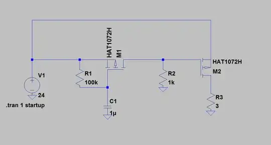
schematic

simulate this circuit – Schematic created using CircuitLab
TonyM
  • 21,742
  • 4
  • 39
  • 62
  • Your calculations are spot-on assuming 5V CMOS output. But the 5V output is said to be TTL, not CMOS, which makes the 5V circuitry output about 4V at most, typically 3.4V with 0.4mA load. I like the idea of external Schottky diode, even if it requires limiting the current below 0.1mA to keep the voltage over it below 0.3V. – Justme May 05 '22 at 21:18
  • I would agree with this proposal if it was TLL 74LS even for TTL with Voh min = 2.7V @ -400 uA and EN = 70% of 3.3 of 2.33V for 0.3V of margin. – Tony Stewart EE75 May 05 '22 at 21:18
  • (+1) This is the safest solution so far, to prevent lockup of CMOS and will draw more current than the internal ESD Sch diodes which have far more series resistance and only rated for ~ 5mA – Tony Stewart EE75 May 05 '22 at 21:58
  • @Justme, I've added a clarification in case OP is using a 1960s chip like LS, though I doubt they are. Please see TTL logic family specs. – TonyM May 06 '22 at 10:32
  • @TonyM I am familiar with TTL logic family specs, and being TTL does not mean same as TTL compatible. For example the HCT you mention is a CMOS chip with TTL compatible input levels and strong CMOS level outputs like HC, so it does not count as a TTL chip. – Justme May 06 '22 at 10:50
  • @Justme, good stuff, I also know something of the history and detail of the families, including the internal circuitry from the handbooks in the days HC(T) was released. However, I don't agree that the terms are used as you describe in practical engineering - the parts and designs that are out there. But that's something for chat, not here, which I'll happily go to if you'd like to discuss further. Meanwhile, I've asked the OP to clarify exactly what part their source signal comes from so we all understand what they meant by TTL for the question. – TonyM May 06 '22 at 16:10
  • @TonyM You have a point, sometimes people say things like "USB to TTL UART adapter" to specify they don't mean "USB to RS-232 UART adapter", even if it's not TTL. Good think you asked for more info. Thanks, I'd love to chat if you wish. – Justme May 06 '22 at 16:48
0

To shift 5V down to 3.3V a simple voltage divider would work. Choosing R1=10k and R2=22k, you'll get a ~3.4V signal, which is within the tolerance of the STWD100NYWY3F. Using the equation Vout = R2/(R1+R2) makes the choice of resistor values arbitrary, but I'd recommend values on the order of 10k so the current draw doesn't get wild.

Edit: As Tony pointed out, the EN pin is pulled down by 36k, so a 80k in series with the EN pin would bring 5V to ~3.4V.

enter image description here

earl
  • 978
  • 3
  • 16
  • The EN signal has internal pulldown of 32k to 100k that will cause variance and margin loss at these values – Tony Stewart EE75 May 05 '22 at 20:29
  • I *could* do this, yes, but the question is whether you can save the 2nd resistor and use the internal protection diode as an alternative method. – nsayer May 05 '22 at 20:41
  • @nsayer I edited the answer to reflect this. Using a single 80k in series with EN should bring your 5V down 3.4V utilizing the internal pulldown resistor in the chip. – earl May 05 '22 at 20:43
  • TTL outputs do not output 5V. They might be near 4V, and typically drop to about 3.4V under 0.4 mA load already. – Justme May 05 '22 at 21:00