1

I'm an electrical engineering student.

The picture below shows a circuit that I found in some old notes but I cannot figure it out.

I have been at it for the last 2 days but to no avail.

Some things that are known for this circuit are:

  1. Beta is close to infinity.
  2. All transistors are the same.
  3. All transistors are in the active region.

I reasoned that since beta is so large, the base current is almost 0. Therefore, it can be ignored. By that assumption the emitter current must equal the collector current. The problem is that I cannot express a relationship that ties Io and all the other currents together.

Could someone please help?

enter image description here

EDIT: Here's what I've done so far.

enter image description here

EDIT No 2: My reasoning on voltage drops.

enter image description here

kosgian90
  • 57
  • 5
  • 3
    What have you considered, already? Where exactly did you find this old schematic? (You are supposed to cite your sources here.) In what context? (There is no way this just comes out of thin air.) And have you thought about temperature effects? – jonk Apr 30 '22 at 19:30
  • @jonk I did not know I was supposed to do all that. It's in some old notes of a class I took. I passed the class a long time ago so I decided to review some of that stuff. The circuit is that nothing else. If my question is inapropriate for some reason feel free to delete it. – kosgian90 Apr 30 '22 at 19:56
  • 2
    Perhaps you could include some of what you just wrote in comments as part of the context for your question? It would help others reading through to have a better idea (and not to ask everything I asked.) I also have old papers I've collected from here and there, though I *always* keep context with them. Schematics like this don't just show up in my notes without some kind of written notes from me and/or other materials to help me understand it years later. But the question isn't inappropriate, so far as I know. It's fine. But you should write down what you've wrestled over and imagine here. – jonk Apr 30 '22 at 19:59
  • @jonk I edited the question. Hope it makes more sense now. – kosgian90 Apr 30 '22 at 20:07
  • I've circled some areas [here](https://i.stack.imgur.com/fQNgG.png). What are these? What's important to know about them? Especially in the sense of, let's say, temperature variation and assuming infinite beta and no Early Effect? Then you might want to imagine what is happening below the green circle and why those two legs might have added below the green circle? – jonk Apr 30 '22 at 20:13
  • @jonk these are standard npn transistors. No particular type or model just generic npn BJTs. In the area that's enclosed with the green circle, I would like to know if any current flows through the base of the transistors. Since beta is almost infinite, i suppose none. – kosgian90 Apr 30 '22 at 20:18
  • Okay. So the green area isn't a recognized "pattern" for you? It is found almost everywhere. So it is a very common pattern. For example, in an answer [elsewhere here](https://electronics.stackexchange.com/a/273901/38098) I can see this pattern in a few places. – jonk Apr 30 '22 at 20:18
  • 2
    It's a current mirror I wanna say. But I'm not sure. It's been a while since i passed the class. – kosgian90 Apr 30 '22 at 20:22
  • 2
    Yes. And how and why does a current mirror *work*? And do you know anything that makes them even more special to use? Something related to temperature variations, perhaps? (Your answers here in comments will help me decide what and how I may respond in attempting an answer. Well, plus the fact that someone else may jump in and help without me needing to write anything.) – jonk Apr 30 '22 at 20:23
  • 2
    Ah it's all starting to come back now. The transistors in a current mirror must be identical. I also think that they are connected in parallel therefore the same voltage drop occurs. So in that way whatever current flows through one's collector must flow through the other's. Right? Also the collector-base junction is shorted on the left hand transistors so they act like diodes. – kosgian90 Apr 30 '22 at 20:34
  • 2
    Yes. Assuming both Q1 and Q2 emitters were grounded, the diode-connected BJT on the left develops a voltage across its BE junction due to its collector current. This sets up a BE junction voltage for the right side BJT, which in response must attempt to find the same collector current. The Shockley equation works both ways: a current develops a voltage, but conversely a voltage develops a current. Of course, in this circuit, the emitters are NOT connected to ground. Something else is going on. – jonk Apr 30 '22 at 20:37
  • The emitters of Q2 and Q3 are connected to ground. However the emitter of Q1 is connected to the collector of Q2 which in turn is connected to Q2's base via short. Therefore it acts like a diode. That's as far as I can go. Could it be amplifying the emitter current of Q1? – kosgian90 Apr 30 '22 at 20:50
  • @kosgian90 The emitters of Q2 and Q3 are NOT connected to ground, but to resistors. Can you write the approximate expression for the current in R1? Then can you find the voltage across RE, and therefore the collector current in Q3? What factor might cause that current to change? – John D Apr 30 '22 at 20:58
  • @JohnD You are right my bad. Changing the resistor value would cause a change in the current. IR1=(VCC-VC)/R1, VRE = VB3 - VBE3. But since the transistors are in parallel, the voltage drop across the CB junction of Q2 and the shorted CB junction of Q1 is the same right? – kosgian90 Apr 30 '22 at 21:21
  • @kosgian90 Can you make an attempt now to start writing down some equations derived from your thinking about the schematic? Something to start with? Anything at all? – jonk Apr 30 '22 at 21:51
  • @jonk I edited the question. – kosgian90 Apr 30 '22 at 22:08
  • @kosgian90 I've responded. – jonk May 01 '22 at 06:06

1 Answers1

3

To Start

Let's start with your diagram and work outward from it.

enter image description here

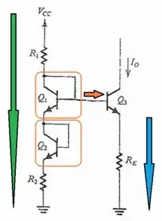
I'll add a few thoughts:

  1. Orange box around diode-connected \$Q_1\$. I'll call the voltage across it \$V_{_{\text{D}_1}}\$ to emphasize its diode-nature.
  2. Orange box around diode-connected \$Q_2\$. I'll call the voltage across it \$V_{_{\text{D}_2}}\$ to emphasize its diode-nature.
  3. \$I_{_{\text{R}_1}}\$: green-labeled current.
  4. \$I_{_{\text{R}_\text{E}}}\$: blue-labeled current.
  5. \$I_{_{\text{B}_3}}=0\:\text{A}\$: orange-labeled current. Obviously zero, since these are infinite \$\beta\$ BJTs.

Development

As \$I_{_{\text{R}_1}}\$ is the same current through \$Q_1\$ and \$Q_2\$ and \$R_2\$ (the green arrow), it follows therefore that \$V_{_{\text{D}}}=V_{_{\text{D}_1}}=V_{_{\text{D}_2}}\$ and \$I_{_{\text{R}_1}}=\frac{V_{_\text{CC}}-2\,V_{_{\text{D}}}}{R_1+R_2}\$.

Now, we know that the base voltage of \$Q_3\$ must be set by the base/collector voltage of \$Q_2\$, which is \$I_{_{\text{R}_1}}\,R_2+2\,V_{_{\text{D}}}\$. Therefore, it also follows that:

$$\begin{align*} I_{_\text{O}}&=\frac{I_{_{\text{R}_1}}\,R_2+2\,V_{_{\text{D}}}-V_{_{\text{BE}_3}}}{R_{_{\text{E}}}} \\\\ &= \frac{\frac{V_{_\text{CC}}-2\,V_{_{\text{D}}}}{R_1+R_2}\,R_2+2\,V_{_{\text{D}}}-V_{_{\text{BE}_3}}}{R_{_{\text{E}}}} \\\\ &=\frac1{R_{_{\text{E}}}}\left[V_{_\text{CC}}\frac{R_2}{R_1+R_2}-2\,V_{_{\text{D}}}\frac{R_2}{R_1+R_2}+2\,V_{_{\text{D}}}-V_{_{\text{BE}_3}}\right] \\\\ &=\frac1{R_{_{\text{E}}}}\left[V_{_\text{CC}}\frac{R_2}{R_1+R_2}+2\,V_{_{\text{D}}}\left(1-\frac{R_2}{R_1+R_2}\right)-V_{_{\text{BE}_3}}\right] \end{align*}$$

Now, I've avoided a few details. The value of \$V_{_{\text{D}}}\$ is actually a function of its current and temperature. So it is really \${V_{_{\text{D}}}}_{\left(I_{_{\text{R}_1}},\,T\right)}\$. Similarly, since all the BJTs are identical, we can say that \$V_{_{\text{BE}_3}}={V_{_{\text{D}}}}_{\left(I_{_{\text{O}}},\,T\right)}\$.

So:

$$\begin{align*} I_{_\text{O}}&=\frac1{R_{_{\text{E}}}}\left[V_{_\text{CC}}\frac{R_2}{R_1+R_2}+2\,{V_{_{\text{D}}}}_{\left(I_{_{\text{R}_1}},\,T\right)}\left(1-\frac{R_2}{R_1+R_2}\right)-{V_{_{\text{D}}}}_{\left(I_{_{\text{O}}},\,T\right)}\right] \end{align*}$$

Sensitivity

The sensitivity equation comes from an easy to understand concept. You may want to know how much something changes when something else changes. But for engineering purposes, you really want to know how much something changes as a percent of its current value when something else changes by some percentage of its current value.

This is expressed mathematically as \$\frac{\%-\text{change}\: P}{\%-\text{change}\: Q}=\frac{\frac{\text{d}\, P}{P}}{\frac{\text{d}\, Q}{Q}}=\frac{\text{d}\, P}{\text{d}\, Q}\frac{Q}{P}\$.

If you know that, you can predict the sensitivity of your instrument. In this case, we'd like to know this: \$\frac{\%-\text{change}\: I_{_\text{O}}}{\%-\text{change}\: T}=\frac{\frac{\text{d}\, I_{_\text{O}}}{I_{_\text{O}}}}{\frac{\text{d}\, T}{T}}=\frac{\text{d}\, I_{_\text{O}}}{\text{d}\, T}\frac{T}{I_{_\text{O}}}\$.

For typical small signal BJTs, the variation of their BE junction voltage vs temperature is anywhere from \$-1.5\:\text{m}\frac{\text{V}}{\text{K}}\$ to \$-2.4\:\text{m}\frac{\text{V}}{\text{K}}\$ (this isn't constant over temperature for a specific device, by the way.) I honestly don't know if there is a standard symbol for this. But let's call it \$k_{_\text{be}}\$. This will have to be calibrated for any given BJT.

So, as an approximation we can say that \$\frac{\text{d}\,V_{_{\text{D}}}}{\text{d}\,T}=\frac{\text{d}\,{V_{_{\text{D}}}}_{\left(I_{_{\text{O}}},\,T\right)}}{\text{d}\,T}=\frac{\text{d}\,{V_{_{\text{D}}}}_{\left(I_{_{\text{R}_1}},\,T\right)}}{\text{d}\,T}\approx k_{_\text{be}}\$.

This allows us to say:

$$\begin{align*} \frac{\text{d}\,I_{_\text{O}}}{\text{d}\,T}&\approx \frac1{R_{_{\text{E}}}}\left[k_{_\text{be}}\left(1-2\frac{R_2}{R_1+R_2}\right)\right] \end{align*}$$

And if we set \$M=\frac{R_1}{R_2}\$, then the sensitivity expression is:

$$\begin{align*} \approx k_{_\text{be}}\frac{T}{I_{_\text{O}}\,R_{_{\text{E}}}}\left[\frac{M-1}{M+1}\right] \end{align*}$$

Worked Example

I just dumped in a model into LTspice and found that \$k_{_\text{be}}=1.75\:\text{m}\frac{\text{V}}{\text{K}}\$, examining temperatures going from \$300\:\text{K}\$ to \$303\:\text{k}\$, for a particular device I'd like to experiment with.

So, at \$300\:\text{K}\$ this works out to:

$$\begin{align*} \approx \frac{525\:\text{mV}}{I_{_\text{O}}\,R_{_{\text{E}}}}\left[\frac{M-1}{M+1}\right] \end{align*}$$

Let's assume that \$I_{_\text{O}}=I_{_{\text{R}_1}}\$ so that the base-emitter voltage differences are the same throughout the circuit. That's probably a helpful idea. And let's assume \$I_{_\text{O}}=1\:\text{mA}\$ and that the base-emitter voltage difference is then \$650\:\text{mV}\$. Finally, let's assume a sensitivity where the first factor (before applying \$M\$) is \$0.5\$, so that \$I_{_\text{O}}\,R_{_{\text{E}}}=1.05\:\text{V}\$ and therefore \$R_{_{\text{E}}}=1.05\:\text{k}\Omega\$. We can also then work out that \$R_2=400\:\Omega\$. (I won't worry, for now, about standard resistor values.)

With \$V_{_\text{CC}}=5\:\text{V}\$, I find that \$R_1=3.3\:\text{k}\Omega\$. This makes \$M\approx 8.25\$ and therefore the fully calculated sensitivity is now slightly less than \$0.5\$, or \$\approx 0.39\$. This means that I should expect to see, for a 1% change in temperature from \$300\:\text{K}\$ to \$303\:\text{K}\$, a change in current going from \$1\:\text{mA}\$ to \$1.0039\:\text{mA}\$. I'll use a collector resistor of \$2.2\:\text{k}\Omega\$. So I'd expect to see a change at the output of \$3.9\:\mu\text{A}\cdot 2.2\:\text{k}\Omega\approx 8.5\:\text{mV}\$.

Here's the LTspice schematic and output run:

enter image description here

The difference is about \$8.32\:\text{mV}\$, which is pretty close to prediction.

There's more to think about. But perhaps this gives a starting point?


I forget to check on the currents vs those used in designing the circuit. Let's look at the currents in the two legs, over temperature, versus the design line of \$1\:\text{mA}\$:

enter image description here

That also looks remarkably good. Keep in mind these are ideal BJTs. But, given that, things appear to work closely to what's expected. Also, note that the magenta curve shows that my estimate of \$650\:\text{mV}\$ is approached only at the higher temperature, \$303\:\text{K}\$, where the currents are exactly as designed. Had I designed for \$\approx 652.5\:\text{mV}\$, the currents would have crossed in the middle of the graph.

jonk
  • 77,059
  • 6
  • 73
  • 185
  • Thank you for the thorough analysis. I have a question though. Since IR is the same current through R1, Q1, Q2 and R2, it is implied that IR=(Vcc-2Vd)/(R1+R2) = (Vcc-Vd)/R1 = Vd/R2. Is that assumption correct? – kosgian90 May 05 '22 at 09:54
  • @kosgian90 No. I think there are both correct as well as mistaken ideas there. Perhaps you could develop your thoughts in your question? – jonk May 05 '22 at 16:43
  • I edited the question. – kosgian90 May 05 '22 at 17:38
  • 1
    The Vcc=Vr1+2*Vd+Vr2 is okay. I don't understand at all how you get Vd=0 from that. I'm not following. The green current is (Vcc-2*Vd)/(R1+R2). True. This is the same value for R1 as for R2, assuming infinite beta for Q3. So Vr1=(Vcc-2*Vd)*R1/(R1+R2) and Vr2=(Vcc-2*Vd)*R2/(R1+R2). – jonk May 05 '22 at 18:12
  • If a DMM was used to measure the voltage drop across R1 what would it show? I'm asking because voltage above R1 is Vcc and voltage below is 2Vd. If no current was flowing through R1 would that hold? – kosgian90 May 05 '22 at 18:22
  • 1
    @kosgian90 In my answer, look at the black chart with the green line for I(R1) -- that's your R3 -- on it. The red line is for I(R3) -- that's your R2. You can see what the currents are. And ***no***! While the voltage above R1 on your schematic is Vcc, the voltage below R1 is ***not*** 2Vd. Where did you get that idea? It's Vr2+2*Vd. – jonk May 05 '22 at 18:43
  • I was just being quite unscientific as it seems. Thank you yet again for your insight. You are really helping me grasp electronics better. – kosgian90 May 05 '22 at 18:49
  • 2
    @kosgian90 It makes me very happy to hear I may be helping. That's the main point for the trouble I go -- to help pay back for those who helped me when I needed it, too. And when I succeed just a little bit everything is right with the world for me. Thanks! And best wishes. :) – jonk May 05 '22 at 18:51