7

Two inputs:

  • Signal: 0-5 volt analog voltage
  • Direction: Standard TTL logic

Output: A single analog voltage from -10 to +10 volts

  • When Direction is low, the Signal is amplified and inverted, so that the original 0 to 5 volts becomes 0 to -10 volts negative.
  • When Direction is high, the Signal is amplified but not inverted so that the original 0 to 5 volts becomes 0 to +10 volts positive.

Low cost and easy construction is more important BY FAR than precision. Positive and negative voltage power supplies are not an issue; +- 12 for example is already available, and other voltage pairs could easily be added.

Any thoughts on how to do that?

James Newton
  • 213
  • 1
  • 6

5 Answers5

7

schematic

simulate this circuit – Schematic created using CircuitLab

The standard configuration that I have used in the past would require two op-amp stages. The first stage is (nominally) unity gain but switchable between inverting and non-inverting. The second stage add the *2 gain that you are asking for.

I'll dig into my old projects and post a schematic.

OA1 functions as a unity-gain buffer when J-FET J1 is OFF. When J1 is turned ON, it functions as an inverter.

The interesting thing about this circuit is that you can adjust the gain of the invert function. Simply adjust the ratio of R2 & R3.

Because the non-inverting mode functions only as a unity-gain buffer, you need to follow this stage with a separate gain stage. One more op-amp and a couple of resistors.

I generally use something like a J175 as the mode FET switch.

Dwayne Reid
  • 23,390
  • 2
  • 35
  • 67
  • 2
    We can't adjust the gain here directly because it would e.g. double on non-inverted by half the gain when inverted? yeah, that makes sense. So invert (or not) on the first stage, then amplify the full range as needed in the second one. – James Newton Apr 29 '22 at 01:00
  • 3
    + and - inputs of the opamp are swapped. – jp314 Apr 29 '22 at 02:59
  • @jp314: many thanks for pointing out my error. Fixed. – Dwayne Reid Apr 29 '22 at 16:09
6

The same arrangement as shown by @Dwayne Reid can be configured to achieve the gain of two in a single stage by adding a single resistor.

R3 is changed to 20k (twice R2) to change the gain in inverting mode to two. Resistor R4 (equal to R3) is added to set the gain in non-inverting mode to two.

The controlling switch is shown here as a P-channel JFET, this has the advantage of being fairly easy to drive with 5V TTL levels. A better option would be an analog switch. A SPDT version that switches the opamp positive input from ground to the input signal would be better still than a shunt switch as shown.

A single MOSFET would not be good with a bipolar input although with the restricted input range from the original question would be ok as the body diode would never be biased on.

Discrete MOSFETs are also not ideal for other than low frequency operation as they have high-capacitance and would not allow the opamp input to faithfully follow the input signal.

This circuit does have its limitations in frequency response and also the noise in the non-inverting mode is increased by the presence of R2 across the input of the opamp.

schematic

simulate this circuit – Schematic created using CircuitLab

Kevin White
  • 32,097
  • 1
  • 47
  • 74
  • Cool..Btw, is there a particular reason for the JFET as opposed to a more usual MOSFET? – tobalt Apr 30 '22 at 05:57
  • @tobalt Presumably it's because of the problem the mosfet's body diode would cause. If the jfet was replaced with a n-channel mosfet then when the mosfet was switched off (gate at 0V), the body diode would conduct when the circuit's input (and mosfet's drain) swing negative, clamping the op amp's positive input at -0.7V. There is no body diode in a jfet. –  Apr 30 '22 at 12:42
3

The simplest approaches that use common parts all use two op amps configured as needed and switching the output between them. To that end, you can:

  1. Use op-amps with a shutdown pin. Those are usually designed for such shenanigans.
  2. Control op-amp supply with an external transistor.
  3. Select the output using an analog multiplexer. The output resistance will be 50-200 ohms depending on what multiplexer mode you use.
  4. Select the output using a homebrew switch.

External output switches can be configured in two ways:

  1. Outside the feedback loop: op-amp’s feedback is taken from the op-amp output pin, and the switch comes after that.
  2. Inside the feedback loop: the op-amp feedbacks are taken from the output after the switch, and the switches are between the op-amp output pin and the feedback network inputs.

The switch-inside-feedback-loop approach will work even with bipolar transistors acting as switches. Using complementary transistors the switches will be bidirectional and pass current going either direction, preserving the output characteristics of the op-amp, with the feedback compensating the C-E voltage and emitter impedance.

Below is an example implementation of this concept.

For optimal performance, the switching cells are current controlled, not voltage controlled. This improves linearity and headroom, so that the output voltages can swing fairly close to the supply rails - this is limited mainly by OA1 and OA2, not by the switches.

schematic

simulate this circuit – Schematic created using CircuitLab

OA1 is the x2 amplifier, OA2 is the x(-2) amplifier. Q1-Q4 are the switches that connect the op-amp outputs to the output node. The feedback is taken directly from the output node. D2 and D3 limit the output swing of the op-amps according to their role. OA1 is limited to 0.5V to +6V relative to the input voltage. OA2 is limited to +0.5V to -11V relative to ground.

R100 is the output load. It is at the edge of what TL071s can drive. When the output load is lighter, the current reference resistor R20 can be increased accordingly.

Q10-Q13 are the current steering control driver, and amplify the 0-5V logic drive signal to +/-12V.

Q20-Q22 form the positive current source, Q23-Q25 form the negative current source. These currents are used to switch Q1-Q4.

Q26-Q29 are differential current steering pairs that route the positive and negative current to either upper (Q1-Q2) or lower (Q3-Q4) switch cell.

R25-R27 form the voltage reference for the current steering differential pairs. R21-R24 adapt the control voltage for current steering use.

And here is its performance:

enter image description here

The switch control currents:

enter image description here

3

Not sure how I missed this (I swear I did search extensively for a match) but this question is basically the same and has a very nice answer: Methods for converting PWM to +/- 10v Signal

James Newton
  • 213
  • 1
  • 6
  • You asked about doing it with two different polarities, ie. you wanted to map 0-5V only to 0-10V or only to 0-(-10V) not both at the same time. That’s a different problem. 0-5V signal has limited resolution, mapping it to +/-10V takes away one bit of resolution. Your question clearly involved switching gains, and thus stands on its own. – Kuba hasn't forgotten Monica Apr 30 '22 at 21:33
  • @Kubahasn'tforgottenMonica. ? He has a switch, I have a switch. it's the same. – James Newton May 01 '22 at 01:05
1

The "standard" solution shown in Dwayne Reid's answer is in fact a virtuoso circuit invented with an ingenious imagination. But to be convinced of this we need to see the "philosophy" behind the specific circuit solution. It will allow us to see the connection with other seemingly different circuits like instrumentation amplifier. Here are some of my observations on the non-inverting mode that can be of greater interest for creatively thinking people.

Internal voltage follower

I have long realized that, including the present circuit, there is a voltage follower inside every (both non-inverting and inverting) op-amp circuit with negative feedback. Its input is the op-amp non-inverting input and its output is the node to which the op-amp inverting input is connected. So the voltage of the inverting input is a "copy" of the voltage of the non-inverting input.

In inverting circuits, the original voltage is zero (real ground); so the copy voltage is zero as well (virtual ground). In non-inverting circuits, the original voltage varies and the copy voltage follows the "original". In the op-amp follower, the copy voltage is used as a circuit output but in other cases it is not used (it still exists but it is not used).

Bootstrapping

In Dwayne's circuit, the original input voltage is applied to the left end of R2 and the copy of the input voltage is applied to the right end of R2. Since the two voltages are connected in series (through the ground) and they are equal and have the same polarity, the voltage across R2 is zero. The current through R2 is zero and the input resistance "seen" from the input voltage source is infinite. This phenomenon is known as "bootstrapping".

Instrumentation amplifier

It is interesting that, in this non-inverting mode, the voltages of all the four points (the input source, op-amp non-inverting input, inverting input and output) are equal. Figuratively speaking, all they "move" in the same direction with the same rate of change.

Even more interesting is the input stage of an instrumentation amplifier…

Instrumentation ampifier

… where, in the common mode, all the six voltages are equal:

Voltage diagram - common mode

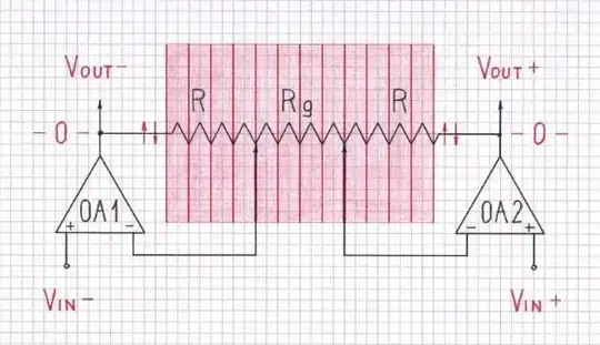
The pictures above are from my Codudact paper about instrumentation amplifier.

Zero gain amplifier

Dwayne's circuit resembles the simplest op-amp differential amplifier where the switch is replaced by a grounded resistor:

Ordinary differential amplifier

The difference is that, at common mode, half the input voltage is applied to the right end of the resistor. As a result, the output voltage stays zero when the common input voltage varies.

So, if you disconnect, connect or short the grounded resistor, you will obtain an amplifier with +1, 0 and -1 gain. You can even replace it with a variable resistor to obtain such an exotic amplifier with a variable gain.

Circuit fantasist
  • 13,593
  • 1
  • 17
  • 48
  • Saying that there is a voltage follower from the non-inverting to the inverting input is very misleading. A voltage follower can sink or source current, but no current flows into or out of the inverting input of an ideal op amp. Analogies are only good if they accurately represent real behavior. This one is just confusing. – Elliot Alderson May 02 '22 at 14:31
  • @Elliot Alderson, I understand you and will explain what I meant. The current is sinked or sourced by the op-amp output through the feedback network, not by the inverting input. I have said "the follower's output is the node to which the op-amp inverting input is connected". The feedback network disturbs the follower and the op-amp increases its output voltage to keep the voltage at the inverting input equal to the voltage of the non-inverting input. So this is a kind of a "disturbed follower". H&H have named this phenomenon "Golden rule" but here I want to explain it more clearly. – Circuit fantasist May 02 '22 at 15:23