I need to generate a +/-12 V square wave, +/-0.4 V tolerance is allowed. The purpose is to drive the pilot signal of an electric vehicle level 2 charger, for those curious.
EDIT (clarification): what I'm trying to design here is the EVSE controller depicted below (the part enclosed in red). As you can see, the output of the circuit is +/-12 V PWM signal in series with a 1 KΩ resistor that is normally open-ended if no car is connected, or pulled to ground through different resistance values by the car to signal different states when it's connected to said car.

END OF EDIT
This is both a hobby project and brain exercise for me, so I would like to use discrete components that I already own, namely BJTs and resistors, while avoiding opamps since the ones that can achieve rail-to-rail outputs within the desired specs are hard to source for me. I'm also aware that a simpler solution would be a MOSFET push-pull stage but as I mentioned before, this is also about trying to understand BJTs better.
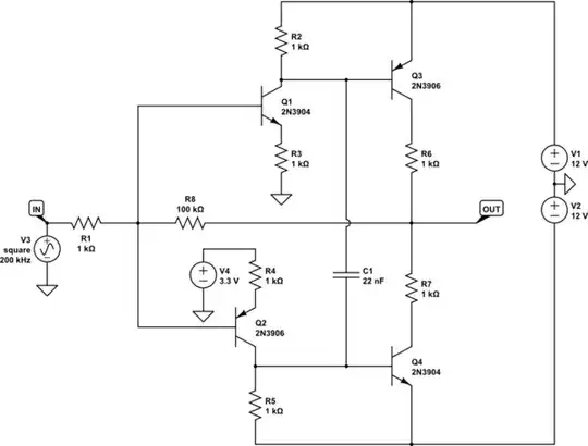
This is the schematic I came up with:
simulate this circuit – Schematic created using CircuitLab
Note that I used a common-emitter push-pull output as opposed to the more usual common-collector because the 0.7 V dropout of the emitter followers would be out of the required specs (+/-0.4 V around rails)
Q1 takes its input signal (0..3.3 V) from a microcontroller and drives Q2 between cutoff/sat.
When IN is 3.3 V, Q2 is off and node A has ~11 V which saturates Q4 while keeping Q3 "almost" off. As a result, OUT has a voltage of -11.8 V, which is well within the desired +/-0.4 V tolerance.
When IN is 0 V, Q2 is on, A has around -11.8 V, which saturates Q3 while keeping Q4 off. In this case OUT shows +11.8 V, which is also good.
However I can see two minor problems:
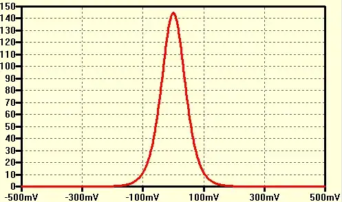
As you can see in the plot below, V(OUT)'s high to low propagation delay is about ~4 µs longer than that from low to high, and I can't really grasp why. As a result, OUT's duty cycle is higher than that of IN so it needs to be compensated from software, which I'd rather not do.
There's some shoot-through current through Q3 and Q4, though not alarming, I'd prefer to not have it. An inductance + fly-back diode might be necessary, but I wonder if this problem is derived from the previous one and fixing it would also fix this.


Simulation of various solutions provided below
For study and comparison purposes. Input is set to 200 KHz to better display propagation delay. Plotted:
- input and output voltages
- \$I_{c}\$ of the output BJTs.
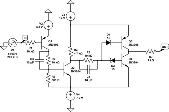
Jonk
This is the currently accepted answer because of its simplicity, low shoot-through and propagation delay symmetry.


This has the problem of both output BJTs being active when IN floats, which could be solved by feedback resistor R8 which latches the circuit in its last status and, additionally, replacing the output resistor R6 with two 1 KΩ between the output collectors.
Also, note: propagation delay symmetry in this circuit depends on the choice of NPN/PNP transistors and, more specifically, their junction capacitances. Try simulating with different transistors or sweeping their capacitances to see the effect.
Hacktastic


Kuba


AnalogKid


