4

I'm trying to teach myself a little bit about BJTs, particularly through the Art of Electronics. I came across something I've been trying for days to wrap my head around. (page 92, third edition)

I cannot for the life of me figure out why the small-signal impedance looking into the emitter is \$ \frac{dV_{BE}}{dI_C}\$. Looking in from where? And if the input voltage is taken to be \$V_{BE}\$, shouldn't the current we're differentiating with respect to be \$I_B\$ instead of \$I_C\$?

Just a note: this showed up right after he introduced the Ebers-Moll model, so this paragraph isn't associated with a schematic. I'm assuming he means this is a law common to all BJTs, irrespective of configuration or biasing.

Would appreciate any insight on this. I'm trying to build a better intuition for BJTs, so any answers that help with that would be greatly appreciated.

Circuit fantasist
  • 13,593
  • 1
  • 17
  • 48
Vortex123
  • 71
  • 1
  • 4
  • https://electronics.stackexchange.com/questions/367321/confusion-about-the-meaning-of-re-and-r%cf%80/367430#367430 – G36 Apr 23 '22 at 22:59

4 Answers4

7

Just follow along:

$$\begin{align*} I_{_\text{E}}&=\frac{\beta+1}{\beta}\cdot I_{_\text{SAT}}\cdot \left[e^{^\frac{V_{_\text{BE}}}{\eta\,V_T}}-1\right] \\\\ \text{d}\,\bigg\{ I_{_\text{E}} \bigg. &= \bigg. \frac{\beta+1}{\beta}\cdot I_{_\text{SAT}}\cdot \left[e^{^\frac{V_{_\text{BE}}}{\eta\,V_T}}-1\right] \bigg\} \\\\ \text{d}\,\bigg\{ I_{_\text{E}} \bigg\} &= \text{d}\,\bigg\{ \frac{\beta+1}{\beta}\cdot I_{_\text{SAT}}\cdot\left[e^{^\frac{V_{_\text{BE}}}{\eta\,V_T}}-1\right] \bigg\} \\\\ \text{d}\,I_{_\text{E}} &=\frac{\beta+1}{\beta}\cdot I_{_\text{SAT}}\cdot \text{d}\,\bigg\{ e^{^\frac{V_{_\text{BE}}}{\eta\,V_T}}-1 \bigg\} \\\\ &=\frac{\beta+1}{\beta}\cdot I_{_\text{SAT}}\cdot \text{d}\,\bigg\{ e^{^\frac{V_{_\text{BE}}}{\eta\,V_T}} \bigg\} \\\\ &=\frac{\beta+1}{\beta}\cdot I_{_\text{SAT}}\cdot e^{^\frac{V_{_\text{BE}}}{\eta\,V_T}}\cdot \text{d}\,\bigg\{ \frac{V_{_\text{BE}}}{\eta\,V_T} \bigg\} \\\\ &=\frac{\beta+1}{\beta}\cdot I_{_\text{SAT}}\cdot e^{^\frac{V_{_\text{BE}}}{\eta\,V_T}}\cdot \frac1{\eta\,V_T}\cdot \text{d}\, V_{_\text{BE}} \end{align*} $$

However, remember that \$I_{_\text{E}}=\frac{\beta+1}{\beta}\cdot I_{_\text{SAT}}\cdot\left[e^{^\frac{V_{_\text{BE}}}{\eta\,V_T}}-1\right]\$ and that the -1 term is ignorable in all practical cases.

So we can simplify and say \$I_{_\text{E}}\approx \frac{\beta+1}{\beta}\cdot I_{_\text{SAT}}\cdot e^{^\frac{V_{_\text{BE}}}{\eta\,V_T}}\$ and therefore substitute that back in to find:

$$\begin{align*} \text{d}\,I_{_\text{E}} &=I_{_\text{E}}\cdot \frac1{\eta\,V_T}\cdot \text{d}\, V_{_\text{BE}} \end{align*} $$

Re-arranging, find:

$$\begin{align*} r_e^{\:'} =\frac{\text{d}\, V_{_\text{BE}}}{\text{d}\,I_{_\text{E}}} &=\frac{\eta\,V_T}{I_{_\text{E}}} \end{align*} $$

We've used derivative calculations to find the local slope near the DC operating point of the B-E junction in active mode and the unit is \$\Omega\$.

For all practical purposes \$I_{_\text{C}}\approx I_{_\text{E}}\$, so you will find either used in the equation. They are close enough for most purposes that you don't need to worry too much over minor details.

Once you find the DC operating point (using other methods), you can work out the local slope behavior when operating at that DC point.

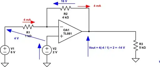
Here's a picture I took from "The Art of Electronics: Student Manual", found on page 101, by Hayes and Horowitz:
enter image description here

That's just to give a "feeling" for the idea. But it is not there when performing a DC analysis. Keep that in mind. It only appears when performing AC analysis around a DC operating point. And it only works just so far and no further than a tiny range around that DC operating point. You cannot apply it over a wide range, because that impacts the DC operating point and you'd need to re-calculate it over and over again, for that. (Re-calculation is what Spice programs do. So they will be good at this. But we humans are far less likely to want to do that.)

To understand why anyone bothers with this, just keep in mind that when a base signal rises upward on the BJT base (let's assume a simple CE amplifier case for now), the emitter generally is supposed to "follow it." But it cannot do that, perfectly, as pulling up on the BJT base tends to increase the collector current. And that means more junction current, which implies a larger base-emitter voltage. So, while the emitter does "follow" the base around, it does so with a slight counter-effect that tends to slightly oppose it. This so-called dynamic-resistance tells you by just how much and it is important in working out active mode voltage gain, for example. Or to use in the linearized small-signal model for the BJT.
jonk
  • 77,059
  • 6
  • 73
  • 185
  • Of course, I agree to everything above. But one comment to the symbol taken from the "Art of Electronics". I heavily disagree to such a symbol. I think, it violates the following general rule: Any symbol which is applicable to small-signal anylyses only (at a fixed DC bias point) must not appear in a circuit diagram (containing the well known transistor symbol). Otherwise, misinterpretations. misunderstandings and calculation errors are probable. Such symbols (re or better gm=1/re) must be used in equivalent small-circuit diagrams only. (See the comment from jonk regarding DC analyses) – LvW Apr 25 '22 at 08:26
  • @LvW The authors of the manual weren't trying to suggest that symbol for the BJT. The student manual chalk-full of cartoon drawings. And that's all it was. A cartoon. I've edited my answer to include a larger context. I probably should have done that, before. My mistake. – jonk Apr 25 '22 at 17:52
  • I think, evreything was already clear in the 1st version of your answer. But back to the "Student Manual" for AoE: Looking at Fig. 6.3 and 6.4 we even see a series connection of both quantities (re and RE) in a circuit diagram.....for my opinion, not a good method for explaining things.... – LvW Apr 26 '22 at 07:50
3

The idea behind this phenomenon is extremely simple; we can name it "virtually decreased resistance".

There is no "resistor re" inside the transistor; just beta times the collector current is added to the base current while the base-emitter voltage is the same. This creates the illusion of the input voltage source at the emitter for (beta + 1) times lower resistance.

The input source is "deceived" because instead of Ib it "sees" beta x (Ib + 1) and "thinks" that the resistance is so low… but this is just an illusion…

So the problem of this common-base configuration, where the transistor is driven from the side of the emitter, is that the input voltage source "sees" a sum of two currents - the input (Ib) and the output one (Ic).

In contrast, in the common-emitter configuration, where the transistor is driven from the side of the base, the input voltage source "sees" only the base current so the input resistance is higher.

So, there is no internal resistance re in series to the emitter. Instead, there is a current source Ic in parallel to the emitter.

If we still are talking about some emitter resistance, it is rather a transresistance since it is a ratio of input voltage and output current variations...

Circuit fantasist
  • 13,593
  • 1
  • 17
  • 48
  • 1
    Thank you for this clarification. I know that in some books and papers the quantity re=Vt/Ic is called "intrinsic emitter resistance". I don`t know why - and there is absolutely no need to define such an "obscure" quantity. In contrast, this definition creates a lot of misunderstandings. This "artificial" symbol re is nothing else than the inverse transconductance gm=d(Ic)/d(Vbe)=Ic/Vt, which constitutes the physical relation between the voltage Vbe and the current Ic. Hence, his quantity gm describes and specifies the most important property of the BJT: Ic=f(Vbe). – LvW Apr 25 '22 at 08:17
  • @Thanks for the support! It is interesting that I still continue thinking about this phenomenon… I think we must admit that this is not an ordinary transconductance as in the common-emitter stage where the input voltage is applied at one place (base-emitter junction) and the output current flows at another place (the collector circuit). Here the current flows in parallel to the input current and is added to it thus creating the illusion of *beta + 1* times higher "input" current. It turns out that the transresistance *gm* is connected in parallel to the resistance *rbe*... – Circuit fantasist Apr 25 '22 at 08:38
0

Due to the current amplification factor hFE or \$\beta\$ the input impedance is lowered by this multiplier so you can say \$r_{BE}= \dfrac{dv_{BE}}{h_{FE} *di_B}\$

This valid for Vbc <0.

For Vce >> 0. Although hFE usually drops ~ 90% when Vbc becomes forward biased as a saturated switch at Vce(sat) approaches 0 @ Ic rated typ. at Ic/Ib=10 for a test value.

Tony Stewart EE75
  • 1
  • 3
  • 54
  • 182
  • In order to avoid misinterpretations and/or calculation errors I like to recommend to use only small symbols (r instead of R) for differentiial quantities which are valid under snall-signal conditions only. More than that, how does the used expression "R_BE" correspond with the question? I think, the ratio d(Vbe)/(d(Ib)*hfe) is identical to the inverse transconductance 1/gm which - sometimes, unfortunately - is called "re". But in no case it has something to do with any resistance between B and E (as your symbol indicates). – LvW Apr 25 '22 at 09:25
0

I'm somewhat at an same early stage in my electronics knowledge, but I think the answer might be quite simple. We are told that the base is held at a fixed voltage. By definition, Vbe = Vb - Ve . If you differentiate all constants disappear. So dVbe/dIc = -dVe/dIc which is re.

Coincidentally, I was only today wrestling with the matter of re (the dynamic, or intrinsic, emitter resistance). Consider a forward biased diode. The current through it is related to the voltage by an exponential formula as below (normalized to make about 10 mA at 0.7 voltage drop). All I did was make up an Excel spreadsheet to calculate re for all voltages from 550mV to 800 mV. It helped me to make concrete sense of re so hope it might be of use to youMy photo

Dabbo
  • 579
  • 1
  • 3
  • 10