0

I would like to use a pchannel FET as a voltage controlled resistor in a circuit where my voltages are between 0 and 1.1 Volts. I'm hoping to use the J175 but truthfully I am having a difficult time even deciphering this datasheet. Am I just tired today?

The two parts making no sense to me right now is Figure 5 showing VGS vs Drain Current and the lines on the graph are also apparently vgs(off) at different temperatures and at different voltages than the voltages of the graph.

Figures 3 to 6

Then there is a given formula in Figure 7. It is rds = rds / (1 - (vgs / vgs(off))).

Figure 7

From the datasheet, vgs(off) can be anywhere between 3 and 6 Volts. I'm just a little lost on how to fill the values into this formula. Obviously I'm wanting to keep Vgs in between 0 and 1.1 Volts and according to figure 12, this can possibly do something - but, how to actually solve.... how to correlate with vgs(off)... I don't understand.

Figure 12

The questions are:

  1. How to correlate Vgs(off) with Vgs in the formula given in Figure 7's formula?
  2. In the formula rds = rds.... Is this to be treated like an iteration (i=i+1)?
  3. If I'm seeing this all wrong, how would you solve for rds?

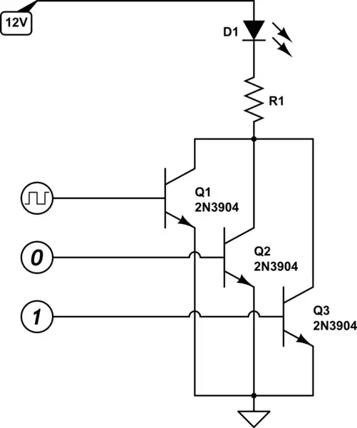
A user asked what problem I'm trying to solve. Here's a small portion of the circuit:
schematic

simulate this circuit – Schematic created using CircuitLab
RobMcN
  • 165
  • 9
  • Which voltages are in the range 0-1.1V? What range of resistance is needed? Why a PMOS? If possible try to avoid the arrangement as the device to device variability is too high to do a good design. What is the problem you are attempting to solve? – Kevin White Apr 20 '22 at 19:21
  • The voltages of my own circuit are 0 to 1.1 volts. I'm happy with a pmos or nmos fet, but in this case I have only 4 FETs, two pch, 2 nch and the j175 has the best rds 'stretch' out of the four. The problem I'm ultimately solving is in a latch circuit. Although I need it to unlatch at a certain voltage (0.65 V), I need it to have a higher resistance until voltage becomes 1. (Hoping 50-100 ohms down to 25 to 10 ohms) – RobMcN Apr 20 '22 at 19:28
  • 1
    Figure 5 reflects the fact there is considerable variability between transistors. The 6 curves show 2 different transistors at 3 different temperatures. Ideally, you design your circuit to be tolerant enough to work well with all 6 of those curves. –  Apr 20 '22 at 20:06
  • @user_1818839 Ok, I'll accept that. What about but what about the formula given in figure 7? – RobMcN Apr 20 '22 at 20:10

1 Answers1

1

With the information given MOSFETs are both temperature and enhancement Vgs sensitive. The device you picked is designed and processed to be a switching device, not a linear device. The On data sheet tells us this: "This device is designed for low-level analog switching sample-and-hold circuits and chopper-stabilized amplifiers. Sourced from process 88." Also remember the parts are designed to meet data sheet specification but they have a guardband and generally exceed the specification. Most data sheets show Min, Typ, and Max for the specifications, not all parameters are filled in. Also not all parameters are tested, many are by design and process dependent.

Gil
  • 4,951
  • 2
  • 12
  • 14
  • Thank you for your thought Gil. Whether or not it is designed as a switching device, it still behaves like a FET and has a resistance at a certain Vgs, Vdd and Id. I also acknowledged in another comment the variability. The questions still stand. How to solve for Rds through testing along with calculations for this device? – RobMcN Apr 29 '22 at 00:19
  • You simply turn it on at whatever Vgs you want, load it with a know current. Measure the source-drain voltage and using ohm's law calculate the resistance. There are other variables that enter into this, mainly die temperature now you can take the manufacturer's specification or purchase the test equipment and measure it yourself. It is easy to do but a lot of work is involved and it changes with each lot of semiconductors. – Gil Apr 29 '22 at 20:05
  • Does no one test a device then use the values to calculate for the values you're actually looking for? I'm looking for a calculated approach to this. I don't mind testing the device and getting its set of peculiar specs, but afterwards I want to calculate specifically for what I want it to do. This should not be beyond electronic engineering. – RobMcN Apr 30 '22 at 01:37
  • A few companies do test devices to be sure they conform to their specifications such as the Automotive but they purchase in large volume and use premium parts. To set up a qualified lab to perform these tests could easily run into multi seven figures cost. The engineering resource perform these tests would also cost a lot of money. The best solution that I and hundreds of thousands have found is purchase from and trust a reputable supplier. – Gil Apr 30 '22 at 15:42