There are many approaches, but I've explored two.
Negative Impedance Converter
OA1 mirrors the R1's voltage drop around the connection point of R1 and R4, effectively negating R1's resistance. OA2 adds this impedance to 450 ohms, and synthesizes it using M1. RPOS and RNEG are the terminals of the virtual resistor.
RNEG can be up to about 5V above the ground. LM324 works fine in this application, as do other op-amps whose input common mode extends to negative supply.
The usual negative impedance converter topology cannot be directly applied, since it terminates the load in the op-amp output. Here, we need both RPOS and RNEG to be free-floating.
V1 and V2 are used for simulation of the effects of op-amp offset.
simulate this circuit – Schematic created using CircuitLab
This circuit has some non-idealities, and can be configured in one of the modes below:
Uncompensated L_COMPENS=0, NL_COMPENS=1e-6: The transfer curve has a slope error, such that the 100 ohm endpoint is raised by R_SENSE.
Linearly compensated L_COMPENS=1, NL_COMPENS=1e-6: The transfer curve has nominal slope, but flattens out a bit before reaching the en.
Non-linearly compensated L_COMPENS=0, NL_COMPENS=1: The transfer curve has accurate endpoints, but its midpoint is lowered by approximately R_SENSE.
Not captured in the schematic is an ideal mode, which suffers none of the tradeoffs of the three modes above. A resistance divider can be used to reduce the effective resistance of R1 by a factor R_SENSE/100 ohm. The cost is an additional op-amp, mosfet, and some assorted discretes.
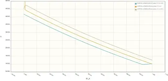
The transfer curves of the uncompensated linear mode (orange) and nonlinearly compensated mode (blue) against the ideal transfer curve are shown below. The green cursor lines denote the error caused by the sense resistance R_SENSE.
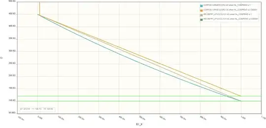
The transfer curve of the uncompensated linear mode (orange) against the linearly compensated mode (blue) is shown below.
Given the application's accuracy needs of about +/-5%, the circuit will work with 1% resistors, and optional trim of the op-amp offset voltages. It is most sensitive to the op-amp offsets. The +/-10mV maximum offset of a low-grade LM324 across temperature affects the transfer curve as follows.
For OP1:
For OP2:
The next largest error source is the nominal value of the R1 rheostat. The 5% error bounds are as follows:
The remaining resistors' 1% tolerances have a commensurate effect, i.e. they introduce at most 1% of error.
The circuit can be readily adapted for bipolar operation, high-side operation, etc.
Reciprocal Resistance Converter
This was my initial approach.
First, a bridge-based resistance multiplier, similar in principle to that one, is used to multiply the 100 ohm fuel gage resistance by a factor of 200x. This virtual input resistance is presented across the MPOS and MNEG nodes.
Then, a bridge-based resistance transformer maps the input resistance range to the output resistance range, presented across the RPOS and RNEG nodes.
With R1 set to 0 ohms, the R_K factor is adjusted to get desired "empty" resistance at the output. Then, with R1 set to 100 ohms, the R_TOT factor is adjusted to get the desired "empty" resistance at the output.
simulate this circuit
LM324 is used only as an example, since its input common mode includes the ground rail, as needed in this circuit. Since relatively low currents are driven through the output resistance, a 5V rail-to-rail op-amp would be sufficient, with a suitably regulated power supply.
The transfer curve is as shown below. It is not linear.
Further development of this scheme would improve the output bridge to be more linear, and/or add a nonlinear element to "bend" the 100 ohm input resistance to linearize the response.
This nonlinear response maps some float assemblies rather better than a linear fit would. The inflection of this curve can be easily inverted as well (upside down).


