2

I designed (with help of several online/offline resources) the following current sink circuit with features:

  1. Should be capable of sinking a maximum of 200 mA (AC, RMS).
  2. Follows the input sine wave V1 of amplitude 359 V at 60 Hz frequency.
  3. POT RV1 controls the amplitude of the current.
  4. Switch SW1 starts or start/stop the current sink.

Current sink circuit

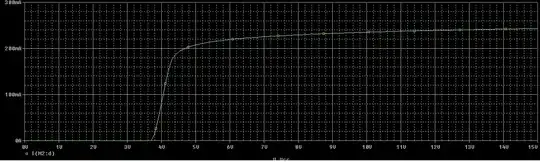
The circuit is working fine as expected. However, when I switch on SW1, an unwanted peak is observed in the current. I suspect that it is because: the base voltage is high at zero current condition. The following figure shows the graph plotted by the oscilloscope. The difference of voltage A and B gives current in mA. The C terminal of the oscilloscope plots the voltage at the MOSFET's gate.

Oscilloscope

Please suggest to me how I can improve my circuit by eliminating the peak. Also suggest me where else I can improve.

Also note that: Irrespective of initial conditions, the circuit reaches equilibrium with gate voltage high.

EDIT: Simplified Circuit is shown here.

schematic

simulate this circuit – Schematic created using CircuitLab

I finally eliminated the SPIKE by adding a 1Mega ohm resitor as shown in the following circuit.

schematic

simulate this circuit

SKGadi
  • 862
  • 3
  • 13
  • 2
    First off, it could be a simulation artifact, something to do with the initial conditions and the internal models. Beyond that, your scope shot does not show either the amplitude or the width of the transient. Please add that information to your question. Integrator U3 has a 22 us time constant, and I don't know how it behaves at startup before the loop is closed. Again, depends on the models. – AnalogKid Apr 15 '22 at 10:43
  • 1
    Questions. What are the input amplitude and frequency? What is the desired output current range? Why is the input signal attenuated through a pot, then attenuated again through an inverting opamp circuit? Couldn't you decrease change R3 to 82.5 ohms, and replace U1 and U2 with a single voltage follower? How did you select the integrator time constant? Adding this information to your question will help with the answers. – AnalogKid Apr 15 '22 at 10:51
  • @AnalogKid, When all the transients are settled, it always reaches the same equilibrium point which is as shown at the initial of the oscilloscope. – SKGadi Apr 15 '22 at 11:10
  • @AnalogKid, I updated the question with sine wave amplitude and frequency. It is 359 V peak at 60 Hz. – SKGadi Apr 15 '22 at 11:10
  • @AnalogKid, Desire output range is 0-200mA – SKGadi Apr 15 '22 at 11:15
  • @AnalogKid, I changed R3 value to 82.5 ohms. Yet, I am receiving the spike. – SKGadi Apr 15 '22 at 11:26
  • @AnalogKid, I cannot join both U1 and U2 because, in the real circuit, I am using several POTs and the U1 acts as an adder. – SKGadi Apr 15 '22 at 11:30
  • 1
    The comment about changing the value of R3 was *only* about eliminating U1 and U2. It had nothing to do with the spike issue. Can you post an expanded view of the spike? – AnalogKid Apr 15 '22 at 14:59

1 Answers1

3

When the SW1 is open, there is no voltage at HVDC, and the opamp U3 still tries to drive Q1 to the specified current (and fails to achieve that) -- it drives the gate fully high. When SW1 conducts, the loop can work as expected.

You need to disable U3 or Q1 when no HVDC is present.

Your circuit might appear to work in simulation because it doesn't include the opamp offsets, but in real life the offsets (esp. U3) will mean that when HVDC is 0 (SW1 open), you can't control what U3's output is.

You could add a small offset to U3 as you did, but it may not be robust in all cases. Better to connect the 1 M, not to the output, but from your 12V supply.

jp314
  • 18,395
  • 17
  • 46
  • I didn't understand where to place the `1M ohm` resistor. – SKGadi Apr 23 '22 at 01:53
  • 1
    Between +12V and the '-' input of U3. It may need to be less than 1 MΩ -- depends on offsets of U1 & U2, and that HVDC is 0 when the with is open. – jp314 Apr 23 '22 at 02:26
  • 1
    You don't need U1 and U2. Connect R4 from the output of R1 to GND, and connect that junction to the '+' input of U3. – jp314 Apr 23 '22 at 02:28
  • If possible, please post the circuit diagram, I am confused with how to place the resist to provide offset. – SKGadi Apr 24 '22 at 13:20