The circuit shown below allows clips the output to +1 and -1. How can I replace the diodes with MOSFETs that have a similar behavior?
-
2Similar behaviour = keep the diodes. – Andy aka Mar 28 '22 at 13:25
-
I know that mosfets connected in a diode-connected configuration can behave like the diode, but I can't seem to find a way to connect them correctly. – Leonhard Euler Mar 28 '22 at 13:30
-
Tie gate to source and use the bulk diode inside the MOSFET. – Andy aka Mar 28 '22 at 13:38
-
An NMOS' body diode has its anode at source and cathode at drain. A PMOS' body diode has its anode at drain and cathode at source. Put an NMOS or a PMOS on each side in a way that the body diodes have the same direction as shown in your circuit. Make sure that each MOSFET has its gate and source are shorted. -- I know, it could be less time consuming if I drew the schematic and put it as an answer. – Rohat Kılıç Mar 28 '22 at 13:40
-
@RohatKılıç, I think it would be very kind of you if you could do that. It would clear matters up. – Leonhard Euler Mar 28 '22 at 13:55
-
@LeonhardEuler are you hoping to use the MOSFETs as "active diodes"? – brhans Mar 28 '22 at 15:46
-
@brhans, yes, that's the intention. – Leonhard Euler Mar 28 '22 at 16:21
-
@LeonhardEuler What is the aim of replacing the diodes with MOSFETs - do you have some control circuitry in mind to switch the MOSFETs on and off? Maybe something like [How do I Implement Soft Clipping in an Audio Circuit? Or should I just Attenuate the Signal?](https://electronics.stackexchange.com/q/87989/36731) is what you're looking for. – Andrew Morton Mar 28 '22 at 16:26
-
Ok - then the suggestions/answers telling you to connect gate to source and just rely on the "body diode" have missed that. – brhans Mar 28 '22 at 16:31
2 Answers
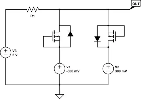
Mosfets have a body diode between drain and source. To use that diode without interference from the channel, you need to keep them off, i.e. set \$V_{\rm GS}=0\$. That's done by shorting the gate and the source. We also need to keep the limit voltages low enough so that the reverse breakdown due to \$V_{\rm GS.MIN}\$ doesn't occur.
I don't see what the point is of using more complex parts in place of the diodes, if all they do is exactly the same, but here you go:
simulate this circuit – Schematic created using CircuitLab
What are the downsides of using the body diode as opposed to real diodes?
They are real diodes. As for their other parameters, such as conductance: you'd have to measure and compare, and first and foremost - decide what's important to you, what sort of performance do you want.
I was under the impression that to get a NMOS to behave like a diode, one needs to connect the gate and DRAIN. Would you mind explaining why such a configuration wouldn't work.
The body diode in a MOSFET transistor is an actual PN junction, and behaves like other PN junctions do: the junction capacitance is modulated by the reverse voltage, the forward voltage is logarithmic in forward current, and so on.
If you connect the gate and drain, you won't have a diode. You'll have a MOSFET that happens to turn on with a couple volts across it one way, and a diode drop the other way - the body diode is still there!
Sure, with low threshold parts, especially ones tweaked to have threshold voltage around 0V, you may get behavior close to a unidirectional ideal diode by using the \$V_{DG}=0\$ connection, as long as you don't expose it to reverse voltages larger than 0.4V or so. But such parts are usually expensive, unless you take off-the-shelf parts and inject enough permanent charge into the gate to move their threshold down to 0V. That's doable, but you'd need to qualify such parts as to longevity etc. It's best to just buy them if you really need them.
The closest you can get to "diode" action with shorted gate and drain would be as below, and even then you still need a reverse isolation diode in series with the channel, so that the body diode doesn't activate. So: an additional diode just to make a mosfet play the role of a diode... doesn't make much sense.
Also note the larger bias voltages, since they have to compensate for the gate-source threshold voltage. The conductance is usually limited by the external diode, except for low-conductance channels typical of CD4007 and older low-signal devices like 2N7000, where the channel itself is limiting. Newer devices have channel conductances that handily beat external diodes.
Diode-based limiters don't have enough gain to do stiff limiting. We need differential pairs for that - even if they are very rudimentary and use only resistor loads as opposed to current sources and current mirrors. In practice, this limiter needs an offset adjustment, but it should otherwise work OK and remain fairly accurate as long as the ambient temperature doesn't change much.
Tying the drain to the gate makes the NMOS behave like a resistor having a voltage drop across it equal to V_TH.
This finds uses in IC design where you will purposefully design a MOS device with a channel width and length selected to get the resistance you need, and thus obtain a resistor. This "diode connection" is not a rectifier!, and it doesn't have the logarithmic characteristic of a PN junction either. It is nonlinear (quadratic) and thus usable for setting up current sources/mirrors and such, since those leverage a non-linear current vs. conduction voltage response of the active device.

- 32,734
- 1
- 38
- 103
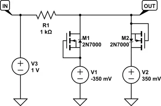
Here's one with using NMOS:
simulate this circuit – Schematic created using CircuitLab
The diodes shown are body diodes. If you short gate and source of an NMOS, it'll turn into a diode. Remember that the forward voltage may differ from MOSFET to MOSFET. So you may need to adjust the other voltage sources.
It's possible to have the same operation with using PMOS. The connection is the same but the body diodes are reversed.

- 26,954
- 3
- 25
- 67
-
Thanks for the schematic. For some reason, I was under the impression that to get a NMOS to behave like a diode, one needs to connect the gate and DRAIN. Would you mind explaining why such a configuration wouldn't work. Also, what are the downsides of using the body diode as opposed to real diodes? – Leonhard Euler Mar 28 '22 at 14:15
-
@Kubahasn'tforgottenMonica, thanks for clarifying that. Is it possible to use a diode-connected configuration to achieve a similar effect. – Leonhard Euler Mar 28 '22 at 14:22
-
@Kubahasn'tforgottenMonica, I'm talking about the one where you connect the drain and the gate together, not the drain and the source. – Leonhard Euler Mar 28 '22 at 14:30
-
Have a look at this figure: https://i.ytimg.com/vi/XO30McD3V8w/maxresdefault.jpg. Typing the drain to the gate makes the NMOS behave like a resistor having a voltage drop across it equal to V_TH. So, I was thinking that if V_TH is approx. 0.7V, I could connect something in parallel with the diode-connected NMOS and also get 0.7V. – Leonhard Euler Mar 28 '22 at 14:42
-
@LeonhardEuler I would highly suggest to actually put one of those things together with an actual discrete mosfet and see how it works. The "diode connection" you refer to is a technique used in CMOS IC design, and is not used as a replacement for diodes. It's a misnomer. The body diode is still there, so the best you get from such a boondoggle is the equivalent of antiparallel connected diodes, or a "bidirectional" diode with somewhat differing conductance each way. Besides, you have **an actual application in mind**: a limiter. Even on an IC you can't make one with diode-connected mosfets. – Kuba hasn't forgotten Monica Mar 28 '22 at 15:04
-
@Kubahasn'tforgottenMonica, can you tell me whether the configuration posted above where we are using a body diode of the transistor as a diode can be used in IC design? – Leonhard Euler Mar 28 '22 at 15:07
-
2Maybe you know this, but in CircuitLab, you can edit the parameters of a MOSFET and change the DISP parameter to ENH_BD to get the body diode to display without explicitly drawing it. Unfortunately, it is displayed as a Zener! (I think the CL programmers confused it with a protection diode. I've reported this issue long ago, but bug fixes on CL seem to be mostly abandoned.) – Theodore Mar 28 '22 at 15:07
-
@LeonhardEuler It can be used as long as there are isolation structures between the substrates of each mosfet thus used. So, most generally, it'd be usable with oxide isolated tubs - where it'd be pointless, since you don't need an entire transistor just to get a diode. Without oxide isolation, you could also leverage parasitic lateral diodes or lateral bipolar transistors as diodes, that arise "naturally" in CMOS circuits. Some discrete power MOSFET switches use such lateral "parasitic" diodes and/or BJTs quite creatively. – Kuba hasn't forgotten Monica Mar 28 '22 at 15:14
-
1@LeonhardEuler a MOSFET with shorted gate-drain will behave like a resistor with an approx resistance of one over gm. The behaviour is like a diode but a bit "softer". So this will show itself as slower response (i.e. longer rise and fall times). Because the body diode is faster. The main application of gate-drain short (diode connected transistor) is to build current mirrors or make pull-ups inside ICs. – Rohat Kılıç Mar 28 '22 at 15:16