6

I have a line-level audio circuit (2-channel balanced to unbalanced input circuit feeding a stereo volume control IC feeding a 2-channel unbalanced to balanced output circuit) which needs a dual PSU (±12V or ±15V). I have some trouble sourcing parts to build an adequate PSU which would fit my space constraints, but I have a couple of 24V DC wall warts lying around - so was thinking I could use a virtual ground / rail splitter circuit to get what I need.

I've done some research (mainly the excellent Tangentsoft article on virtual ground circuits and a couple of EE.SE questions, e.g. this one).. and I promptly ran into issues sourcing parts for the more common types of circuit (TLE2426 + BUF634, neither of which I can easily buy), so I figured I'd try another approach: combining the feedback topology of an op-amp based virtual ground with a discrete transistor buffer to get greater current capability. Based on the aforementioned article and another article which deals with buffering op-amps for higher current I came up with the following circuit:

schematic

simulate this circuit – Schematic created using CircuitLab

I opted for NE5532 simply because I have a few of them lying around. My question is - unless this is completely the wrong idea - will it work? Won't it oscillate like crazy due to the "dead band" between -0.7V and +0.7V, where the transistors are in cut-off?

I only dabble in electronics, so I apologise in advance if this is completely bonkers..

devnull
  • 8,447
  • 2
  • 15
  • 38
Dan Kadera
  • 69
  • 2
  • 1
    This works well current limited by slew rate and hFE gain with the right choices of components to drive the necessary load and the oscillations can be filtered by a large ferrite bead after the output. – Tony Stewart EE75 Mar 24 '22 at 15:04
  • 4
    Fit a 220 ohm resistor between base and emitter and let the op-amp do the little punches. – Andy aka Mar 24 '22 at 15:09
  • This will work well for low (a few tens of milliamps) load currents. I don't know what the current requirements are for each rail but I'd like to add that if you try to draw too much current (something larger than a few hundreds of milliamps) then the balance will be lost i.e. the rail voltages will not be ±12V (e.g. +18V/-6V or +3V/-21V, depending on the currents drawn from each rail). So if you want higher currents you need to add more totem-pole output stages. But, as I said, this totally depends on the load current requirements. – Rohat Kılıç Mar 24 '22 at 15:23
  • Thanks for the tips guys, but - sorry - a bit of a noob here ;-) @TonyStewartEE75, the NE5532 has a slew rate of 9V/us iirc and the 2N3904 / 2N3906 BJTs have a hFE around 100, would that be ok? And where would I put the ferrite bead, on all three output wires, or just the ground? – Dan Kadera Mar 24 '22 at 15:27
  • 3
    And @Andy aka, do you mean basically between the OPA output and the VGND? So iiuc small deviations on VGND / small currents would be handled by the OPA and larger ones by the transistors? – Dan Kadera Mar 24 '22 at 15:28
  • @RohatKılıç the load is a circuit with 5x NE5532 (which should draw 20mA max each) and a single PGA2310 (which should draw 10mA max), so I'd estimate the total max current draw at less than 150mA. – Dan Kadera Mar 24 '22 at 15:32
  • @Andyaka "220 ohm between base and emitter", I didn't quite get that. You talk about the BJTs right? The "between" base and emitter is inside the BJT. Where do you suggest the resistor to be placed? – Christianidis Vasileios Mar 24 '22 at 15:36
  • 1
    @ChristianidisVasileios well, you can't fit them inside can you. – Andy aka Mar 24 '22 at 15:38
  • *"a circuit with 5x NE5532 (which should draw 20mA max each)*" Less than that if you consider that the BJTs only need to handle the imbalance. If you connect the opamps power supply pins to +12V and -12V, some of this current will not flow to/from vgnd. – devnull Mar 24 '22 at 16:01
  • 1
    @devnull yeah, I was thinking more in terms of absolute maximums instead of typical operation – Dan Kadera Mar 24 '22 at 16:07
  • 1
    **It is impossible to design such a circuit without knowing the total capacitance between each rail and VGND**. The compensation and transistor gain and transconductance requirements will all depend on the load capacitance. Without it, it's garbage in = garbage out. Whatever you design will not work, because you're not designing for the load you have in mind. You also need to specify the test load current waveform (e.g. square/sine wave, frequency and amplitude), and the maximum allowed transient voltage deviation from the middle. Can't design anything without it either. – Kuba hasn't forgotten Monica Mar 24 '22 at 21:51
  • 1
    Keep in mind that many power supplies have rather disappointing or under-specified transient response, so if you're designing something yourself, you need to have the specifications in mind first: average load current, maximum positive and negative load current, complex load impedance (or explicit capacitance and ESR), regulation bandwidth of interest, allowed transient response amplitude for a line and load transient of a given amplitude, and so on. Figure out what you want first. And only then you can think of designing anything. It's a waste of time otherwise. – Kuba hasn't forgotten Monica Mar 24 '22 at 21:53
  • 1
    I can toss a dozen designs here that will all work for some load impedance and transient response requirements, but I doubt very much that any of those will be exactly what you have in mind. You're designing an application-specific supply for audio use, so perhaps start by feeding some test signals into your load, and measure the AC currents that flow through the "ground". For that you'd need a current amplifier shunt with sufficient bandwidth, eg. something like uCurrent. – Kuba hasn't forgotten Monica Mar 24 '22 at 21:56
  • This is an internal slew rate limiting problem. No excuse for contrary errors from you guys – Tony Stewart EE75 Mar 24 '22 at 22:51
  • **You should avoid Active Split Supply designs** for audio power and instead use single supply differential mode to eliminate the ground current losses and draw directly from the supply and return rather than thru the added small BJT's Beware there are false opinions in this thread from others. This will reduce your efficiency another 50%. – Tony Stewart EE75 Mar 24 '22 at 23:23
  • 2
    @Kubahasn'tforgottenMonica I suppose I'd understand at least some of what you're suggesting had I majored in circuit design; unfortunately I was in sound design and even that I dropped out of.. so while your suggestions are much appreciated (no sarcasm!), they aren't practically applicable for me. I could post the schematic for the whole load circuit, but I don't want you guys to do my work for me, and apparently this is way above my skill level.. I'll experiment some more, but unless I get lucky I suppose I'll have to dish out for an expensive ready-made solution in the end.. – Dan Kadera Mar 24 '22 at 23:25
  • 2
    @TonyStewartEE75 I'm not all too worried about efficiency - as I said, the load is a _line-level_ audio circuit - basically a fancy volume control to sit between, say, a sound card and a power amp - so from an efficiency standpoint, I don't care much if it consumes the "optimal" 120mA or 250mA due to inefficiencies. Also the load circuit is already done and tested and it _requires_ a dual supply and there's little I can do to change that. – Dan Kadera Mar 24 '22 at 23:39
  • YOu ought to improve your question and measure the ground current as a design spec. and include a ripple spec for max signal voltage at max frequency. – Tony Stewart EE75 Mar 24 '22 at 23:47
  • @TonyStewartEE75 that'd require me to buy the uCurrent or something similar, wouldn't it? Which means more $$$, more weeks waiting.. No. Sorry, can't do it. I thought a rail splitter would be a pretty simple thing, but apparently it's closer to rocket science than I thought. – Dan Kadera Mar 25 '22 at 12:17
  • No you just insert a resistor to measure say a 50 mV drop to measure current or perhaps an ammeter, If small this could be trivial without the need for BJT's – Tony Stewart EE75 Mar 25 '22 at 15:42
  • As this Q&A has degenerated into accusations and unfriendly comments (which have been deleted - note that the code of conduct applies to what people write to mods too!) I'm locking the whole Q&A while considering the next actions and to give time for people to calm down. || Update: 2022-03-26 17:27 UTC The topic has now been unlocked. – SamGibson Mar 26 '22 at 01:33
  • 2
    @DanKadera please explain what the maximum current draw from the pos rail is when current from the neg rail is at its lowest. This indicates the imbalance forces that need to be countered in order to maintain a steady mid-point rail. Ditto for the neg rail when the pos rail current is lowest. We'll then have the full picture of the AC current that needs to be supplied by the mid-rail generator. Also, state what the loading capacitance is on the mid-rail as that could cause instabilities quite easily. If you can't supply these details then it's guesswork. Frequencies of current are also useful. – Andy aka Mar 26 '22 at 19:24
  • Late to the party, but still ... The net GND current is the algebraic sum of all of the individual stages GND current. Do you have an estimate for the amount of ground current the circuit will have to source/sink? If some of the signal stages are inverting, their GND current is at least partly cancelled by stages that are not. It is entirely possible to have 20 signal stages and only 5 mA of net GND current, something that can be supplied by the opamp with no booster stage. – AnalogKid Mar 31 '22 at 12:35

3 Answers3

12

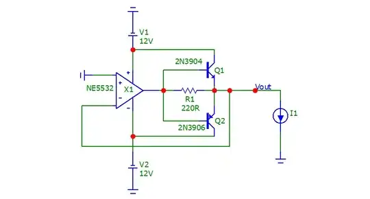
This is what I suggested as a comment a couple of days ago: -

Fit a 220 ohm resistor between base and emitter and let the op-amp do the little punches.

So, what does the output voltage look like when we discard the BJTs and connect the op-amp (via a 220 Ω resistor) to a 1 kHz sinewave of 10 mA peak-to-peak: -

enter image description here

The output ripple is about 0.3 mV p-p but, is this too much? It might not be too much for many applications but, that's for the OP to decide. Of course, there are other tricks that can be done but, the main focus now is to show the clear benefit of adding a 220 Ω resistor (as previously mentioned). Maybe I'll add more additions in a day or so when the OP provides more detail.

Recap - I'm not trying to solve the OP's overall problem because, without full details of the load that's guesswork. However, the OP has been asked (in a comment under the question) this: -


@DanKadera please explain what the maximum current draw from the pos rail is when current from the neg rail is at its lowest. This indicates the imbalance forces that need to be countered in order to maintain a steady mid-point rail. Ditto for the neg rail when the pos rail current is lowest. We'll then have the full picture of the AC current that needs to be supplied by the mid-rail generator. Also, state what the loading capacitance is on the mid-rail as that could cause instabilities quite easily. If you can't supply these details then it's guesswork. Frequencies of current are also useful.


As soon as numbers are provided, an attempt will be made. However, at this moment, I'm trying to show the clear benefit of fitting a 220 Ω resistor between base and emitter. Read on please...

So, the above is what you will get for light current load variations when that demand is small to moderate i.e. before the BJTs can bring anything much to the party.

Why did I choose 10 mA p-p ripple current (I here someone ask)?

I chose a 10 mA p-p ripple current because, at this level, the peak to peak voltage on the true op-amp output would be just about starting to activate the BJTs should they be fitted. If the output current ripple were any greater, then the BJTs would start to do the heavy lifting and we'd not recognize how useful the 220 Ω resistor can be.

So, just for clarity, here's the true output of the op-amp when feeding the mid-rail net via a 220 Ω resistor connected to a 10 mA p-p ripple sinewave of 1 kHz: -

enter image description here

As you can see, the true op-amp output voltage peaks are hitting a little higher than the nominal +/- 0.7 volts i.e. they would just be starting to properly to activate the BJTs (should they have been connected).

And clearly, we are not taxing the op-amp at all. In fact it could handle a load ripple current of about 20 to 30 mA p-p (as opposed to 10 mA p-p). So, I'm not asking the op-amp to do much here. But it won't handle much more. However, it doesn't need to because that's when the BJTs will be doing the heavy lifting (when fitted). Here's what happens when they are fitted (with a load ripple of 100 mA p-p): -

enter image description here

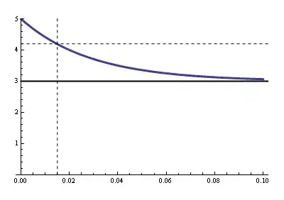
The above is the mid-rail output voltage with a load ripple of 100 mA p-p. The ripple voltage is about 2.9 mV p-p. It's not bad but, for audio applications it might just be too much. With a load of 200 mA p-p ripple current we see this: -

enter image description here

The ripple is about 5.5 mV p-p. But, here's the rub...

If I removed the 220 Ω resistor to mimic the OP's original circuit idea (same load ripple of 200 mA p-p) we see an output ripple voltage of about 450 mV p-p i.e. about eighty times more ripple: -

enter image description here

This is why I suggested adding a 220 Ω base-emitter resistor because it's a no-brainer. Circuit with the 220 Ω resistor fitted: -

enter image description here

Remember, I'm trying to show the benefit of adding 1 resistor to the OP's circuit.


But, you could also bias-up the BJTs a tad and turn your class B stage into a class AB stage: -

enter image description here

So, flowing through each BJT is about 6.8 mA DC due to the little bit of biasing applied with the extra resistors. Here's what the ripple looks like with a 200 mA p-p load: -

enter image description here

It's about 0.15 mV p-p and might possibly be good enough for the OP's application. Notable is that if I remove the original 220 Ω resistor (R1 above), the ripple remains about the same.

So, the options are: -

  • Use R1 with no BJT biasing (class B) to get a ripple of about 5.5 mV p-p
  • Don't use R1 to get a ripple voltage of about 450 mV p-p (yuk)
  • Bias the BJTs (class AB) to get a ripple voltage of about 0.15 mV p-p

Also remember that if there is capacitive loading (probably quite likely) then some effort will need to be made to prevent the op-amp from turning into an oscillator. However, quite often with op-amps circuits like this, if you "over-power" the output with a significant amount of capacitance then the op-amp comes back into stability. It's roughly the 1 nF to 10 μF region of loading capacitance that can turn a linear amplifier into an oscillator and, that must be totally avoided.

So, with a 10 μF "smoothing" capacitor added to the output, the circuit will "sing": -

enter image description here

But, if the op-amp part has a localized 100 pF feedback capacitor, you get a stable result: -

enter image description here

But, because you have de-graded the op-amp performance with the 100 pF localized feedback capacitor (in order to stop it being unstable), you have also de-graded its ability to counteract ripple from the previous level of 0.15 mV p-p (no output capacitance and no localized feedback) to 0.85 mV p-p (10 μF output capacitance + localized stabilizing feedback). Circuit with 10 μF output capacitor and localized feedback capacitor: -

enter image description here

So, it's a fine balance that you need to make when you add capacitance to the output. It may be that with a 10 kHz ripple-current loading on the output (previously 1 kHz), the balance swings to adding an output capacitor so that it does the heavy lifting rather than the op-amp and BJTs.

Andy aka
  • 434,556
  • 28
  • 351
  • 777
2

I have a couple of 24V DC wall warts lying around

If other options besides the rail splitter are to be considered, why not use two SMPS working independently as buck and inverted buck-boost?

This is just an example, working at a switching frequency of 520 kHz. Two of these DC-DC converters could be connected like this:

enter image description here

To be clear, two different SMPSs are not required. You could derive both circuits by connecting two buck converters differently. As explained here

enter image description here

and even here:

enter image description here

devnull
  • 8,447
  • 2
  • 15
  • 38
0

The circuit you have is not representative of how it'll be used.

To simulate it, try some 4MHz op-amp like TL081, and add load capacitance, say 100uF with 20mOhm ESR between VGND and both other rails. Then add some AC load current, say 50mA amplitude at 5kHz. Then observe the behavior of the circuit.

Since the transistors don't conduct on crossover, the circuit then runs open-loop and the internal nodes in the op-amp charge up and take a while to get back into balance once the opposite transistor starts conducting. Thus, every time the load current changes direction, the VGND voltage jumps by quite a bit - tens of mV, easy. This will be clearly audible.

You need a circuit that keeps both transistors biased on, with some idle current - say 10mA. Such circuits are more involved than they may look like. The transistors you're using may have current gain and power dissipation too low for this application - you need to decide how your load looks, and design for that.

I suggest just not doing this. If you want split supplies, use a ready-made isolated power converter brick that takes, say 12V or 24V on the input, and puts out regulated +/-15V or +/-12V. Those can be found on eBay. You can also use two 24-to-12V bricks, with inputs in parallel and outputs in series. Since the outputs are isolated, they are floating voltage sources and can be stacked on top of each other, etc. That'll be the simplest solution for a one-off.

  • The crossover distortion is internal slew rate limiting and not bias current starved BJT's . This is clearly false. Adding bias current or even Class A will not speed up the internal slew rate of an op amp. Choosing a faster one will. -1 I hope you stop and understand before you reject this fact overlooked by everyone else. – Tony Stewart EE75 Mar 26 '22 at 01:14
  • @TonyStewartEE75 Well, of course internal slew rate limit is a problem when you'd need an infinite slew rate to cross the cutoff region of the VBE without losing control of the output. If the constraint is that at least one transistor conducts, then with the bases shorted together, you'd need an infinite slew rate. So that's not very helpful - you'll only achieve "continuous" conduction when the op-amp will slew faster than the transistors can switch. A BE resistor will provide a conduction path bypass, or a voltage source between the two bases, to maintain crossover bias. – Kuba hasn't forgotten Monica Mar 27 '22 at 00:03