2

I designed a +/-15V power supply setup and trying to find/fix problems before running another PCB production run.

It will accept 36VDC (800mA) from an off the shelf part via a barrel connector. I cannot change that part of the equation so I'm trying to desing something around that thing.

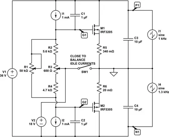
My current layout looks like the following picture: enter image description here I plan to use a buffered voltage divider which in turn controls a pair of n-channel and p-channel MOSFET's to provide enough power for the following linear regulators.

I'm aware of possible oscillations due to the capacitive load on the op amp, I ran some SPICE simulations and found the values in the schematic for sufficient. Here are some screenshots of the measurements with and without the compensation: Without compensation enter image description here

I selected these parts here:

I ran a (quite simple) simulation in circuit.js if anyone wants to follow my train of thought and how I even got here.

My question after this huge preamble is the following:

Am I completely on the wrong path with my idea here or is there a chance of this thing working?


EDIT:

  1. If there is any large power imbalance in loads, then the driver transistor will dissipate the difference in Watts. i.e. for audio it would be < 50% efficient. If so, the design would be better with differential output driver from single supply.

This answer by Tony Stewart EE75 brought me to the conclusion, that trying to supply power that way isn't feasible in my case and instead I'll go down the road of modifiyng the main circuitry to work with a single-rail supply rather then force that concept of having a positive and negative supply.

Khanorr
  • 35
  • 4
  • How much current does the load need? Maybe there is a simpler architecture based on that. – Aaron Mar 21 '22 at 18:28
  • You may want to add this comment you made on the previous question to this one: *"This is (sooner or later) going to replace a now obsolete power supply element which is driving an analog device (audio switching/volume) and is designed around a pretty clean +/-15V supply. That's also the reason why I planned to use linear regulators instead of buck/boost stuff to minimize noise coupling into the audio paths. There's also an integrated amp that draws around 220mA under full sine load on each supply rail, so charge pumps and such are also not an option."* – devnull Mar 21 '22 at 18:39
  • Does the 36 VDC come from a shelf part based on a rectifier + capacitor filter? If this is the case, why the tiny ripple (100 or 120 Hz) which will appear after the regulator is not an issue but the ripple at hundreds of thousands of Hz and above from two SMPSs is a problem for the audio circuit? – devnull Mar 21 '22 at 18:43
  • 1
    Bad idea for 30W with an active split supply ground – Tony Stewart EE75 Mar 21 '22 at 19:21
  • @denvull I ran tests with a few SMPS and the audio circuitry had some layout issues where switching noise would be coupled into the signal and get audible. The tiny ripple around 100Hz (in my case) wouldnt be a problem since it doesn't have the energy (or rather the changes between positive and negative are slow enough) to not cause an issues whatsoever. – Khanorr Mar 22 '22 at 11:30
  • The point #3 only applies to your circuit taken literally with decoupling capacitances that are 2-3 orders of magnitude too small. As soon as you put reasonable decoupling capacitors in place, e.g. 1-10mF from each rail to center/common, it won't be a problem, since AC currents won't flow through the mosfets. But in this application the 7815/7915 regulators won't work. You need LDO types that drop off 1.5V or less. You don't have 3V of dropoff - such ideal conditions are a fantasy. – Kuba hasn't forgotten Monica Mar 22 '22 at 19:02

4 Answers4

2
  1. 1st problem is lack of design specs. for Min/max load impedance and imbalance range. ripple and step load error.

  2. FETs have too much nonlinear gain and C3 causes oscillations.

  3. If there is any large power imbalance in loads, then the driver transistor will dissipate the difference in Watts. i.e. for audio it would be < 50% efficient. If so, the design would be better with differential output driver from single supply.

  4. BJT's would offer lower gain and better transient load stability.

Other than above, I might suggest either a Class AB design or this

simulation schematic

SamGibson
  • 17,231
  • 5
  • 37
  • 58
Tony Stewart EE75
  • 1
  • 3
  • 54
  • 182
  • Thank you, your remark with a differential output driver brought me back on the right path here. The whole circiutry that this should be supplying is already using differential recievers and drivers anyway. So instead of trying to supply power through this, I'll think I just use it (without FET's, BJT's or else) as a buffered reference and use the full 36VDC as single supply for the whole thing. Thanks again for your time! – Khanorr Mar 22 '22 at 11:35
  • Re. your point #3: The AC current should be flowing through decoupling capacitors anyway, and only a small ripple current should be flowing through the mosfets. So that's not a problem in a well designed circuit. Presumably the audio stage would be push-pull into a center-referenced speaker. The DC current through the mosfets should be in tens of mA, just biases and quiescent current imbalances. The AC current should be bypassed. – Kuba hasn't forgotten Monica Mar 22 '22 at 19:00
  • @Kubahasn'tforgottenMonica Its not the DC, but the AC Pd in this class that is inefficient with active ground similar to the Class AB driver – Tony Stewart EE75 Mar 22 '22 at 23:39
0

Because of the get threshold voltage of your mosfet, the system will oscillate like crazy. You can filter after that but as we say, garbage in garbage out.

You need some circuitry to drive the mosfets gates in the linear region, which means offset each of the gates, and have a small bias current flowing through them.

Some mosfet audio amplifier does that.

Doable, but why not just use buck converter to go from 36V to 15V and then use a charge pump inverter like the SI7661, which are actually done for that purpose and will have much better efficiency.

SamGibson
  • 17,231
  • 5
  • 37
  • 58
Damien
  • 7,827
  • 1
  • 12
  • 29
  • That was something I was worried about and one of the things I never designed before, that's why I posted it on here. This post and the answers to them is worth more than scouring the net for a few hours and still have no definitive answer. – Khanorr Mar 22 '22 at 11:52
0

One thing that you need to do is run an AC analysis and test the stability of the reference as it looks stable at DC, but an audio supply needs to be able to source and sink current from the reference ground at audio frequencies. The reference ground might not have much stability at certain frequencies. It really depends on how much current will be dumped on the reference ground.

It might be difficult to get it to work as an analog/audio supply, but that really depends on how tolerant of noise the analog electronics need to be.

Voltage Spike
  • 75,799
  • 36
  • 80
  • 208
0

The idea is workable, although 3V dropout for those 78/79 regulators is marginal, especially if the 36V supply is not very accurate. You should use LDO types instead.

The controller you propose loses control of the reference voltage when both mosfets turn off. This will cause problems whenever the load current reverses direction.

Instead, a simple circuit could be used as a pre-regulator, using the gain of just the mosfets. It will maintain the reference voltage about +/-0.5V from the midpoint. This circuit maintains a bias current across the mosfets, so that as the control passes between M1 and M2, there's never a case when both are off.

R1 sets the total idle/bias current. R3 balances the bias current between M1 and M2. These should be adjusted with SW1 closed.

C3 and C4 are not just 0.33uF, because that's the minimum value needed for stability of the 78/79 regulators you chose. It's nowhere near enough if you want to have best possible line and load regulation. 10uF is better, 100uF would be even more so. The 0.1uF C6/C7 in your schematic are laughably small. 100uF would be a minimum. Yeah, 100nF is OK to stabilize the regulators, but their load regulation will be poor.

An additional gain stage could be added to amplify the difference between VREF and 18V, feed that to the wiper of R3. C1 and C2 would then be connected between R3 wiper and mosfet gates.

schematic

simulate this circuit – Schematic created using CircuitLab

SamGibson
  • 17,231
  • 5
  • 37
  • 58