3

While tuning a 12.5 MHz 3.3V signal (square wave expected 3.3V to 0.0V,) I am seeing overshoot reach of +5.0 V and negative overshoot of -2.0V. I am intentionally not using the term undershoot here as my understanding of undershoot is when my signal is not able to reach 0.0V.

I read about overshoot and undershoot definition and causes, basically unmatched impedance and reflections, and some practical suggestions to mitigate this using a series resistance R (33 ohm to 120 ohm) or using a RC filter will also help in arresting the overshoot and undershoot.

Actual Waveform

Actual signal

Then I started tuning with an RC filter, 33ohm and 220pf

33ohmand220pf

Next try with an RC filter, 33ohm and 100pf** to reduce damping

33ohmand100pf

When I mounted the RC filter on 22 signal lines the cumulative effects all together were again corrupting the signal quality.

I made one last attempt, and removed all the capacitors and only mounted series resistors of 130 ohm.

series130ohm

Now coming to the actual question, why do we see these positive and negative overshoots?

My understanding is that a square wave is made of multiple sine waves overlapped together, which will also have odd harmonics occurring at (3 X frequency), (5 X frequency) and so on. ( Follow the SE link for more details.) As my signal frequency is 12.5 MHz and if I design a low pass RC filter of 12.5 MHz with the intention to filter all the harmonics out of my circuit, will it solve the problem?

RC

I think I am not completely correct here, something is missing. If I just use a conventional solution of 120 ohm series resistance, the results are promising as seen in last waveform. Yes, I also know I can go for simulation using LTspice or other EDA tools, but I am looking for the actual cause.

JRE
  • 67,678
  • 8
  • 104
  • 179
AKR
  • 2,273
  • 4
  • 22
  • 34
  • 1
    What is your source impedance 0? how long is 10:1 probe ground lead? my guess 30 mm – Tony Stewart EE75 Mar 16 '22 at 06:44
  • Did the measurements using GND spring, no cables, probe setting 10:1 – AKR Mar 16 '22 at 06:58
  • Resonance at 85 MHz suggests you have parasitic inductance with Q ~ 3 on a 1st order LPF with low source impedance =? – Tony Stewart EE75 Mar 16 '22 at 07:07
  • my simulation https://tinyurl.com/y7vebcvc – Tony Stewart EE75 Mar 16 '22 at 07:20
  • 1
    Please note that the waveform is something that the scope sees, or rather, what your probes pick up. It's not necessarily the waveform the oscillator outputs. Which oscilloscope you are using, which probes, are probes on 10x setting and is there a huge length of crocodile clip ground wire or low impedance ground spring for probe grounding? Post a picture of the setup. – Justme Mar 16 '22 at 07:21
  • There are too many assumptions you are making in your equivalent circuit that are missing and your photo's too... as you can see by my simulation – Tony Stewart EE75 Mar 16 '22 at 07:32
  • 1
    first thing, as already suggested check your probe setup. In https://electronics.stackexchange.com/questions/411399/how-the-low-inductance-of-short-ground-clip-probes-prevents-interference the second image shows the correct accessory to use – Lorenzo Marcantonio Mar 16 '22 at 07:33
  • 1
    his 1st comment confirmed gnd spring – Tony Stewart EE75 Mar 16 '22 at 07:34
  • Then we should look at his oscillator output stage, it could simply be a snubberable ringing (across the switch, not on the output) – Lorenzo Marcantonio Mar 16 '22 at 07:35
  • With 3.3V into a 33 ohm load source impedance does not look like ordinary CMOS , bad assumption or information – Tony Stewart EE75 Mar 16 '22 at 07:36
  • resonance about 75 to 85 MHz on 1st plot what the equivalent L will be – Tony Stewart EE75 Mar 16 '22 at 07:38
  • @TonyStewartEE75 sorry not able to access the simulation using office machine, and can you please also guide me how do you see resonance at 75 to 85 MHz. I am not able to figure it out, seeing my waveforms. – AKR Mar 16 '22 at 10:04
  • I was also looking for explanations why I am getting these overshoots, also in general why do we get overshoots in signal. – AKR Mar 16 '22 at 10:06
  • Try this at home https://tinyurl.com/y9bflaqz – Tony Stewart EE75 Mar 16 '22 at 17:00

1 Answers1

5

Overshoots and ringing are a sure sign of second order effects.

It may be from +j reactance (L inductance) with -j or C, capacitance or in Active ccts, positive feedback or lack of gain margin in active feedback. (pick 1 or more causes) See my Simulation. On breadboards , it can be due to both L and lack of C near IC.

  • We call parasitic R in caps as ESR and inductance as ESL (effective series inductance.)

It may be 2nd order or higher depending on the number of loops in your circuit. Inductance depends on conductor geometry and ln (l/d) in [nH/mm] but tends to vary around 8 nH/ cm +/- x%.

  • Parasitic capacitance also depends on geometry but by ratio of area and gap,x or ratio of a/x .

    • For example: Finger almost touching = 1pF ( my calibrated finger ;) but just touching ~ 100 pF from ESD HMD model and measuring with DMM R = 1M to 10 Meg but with an ionized arc R ~ 100 ohms is used for ESD model.

enter image description here

enter image description here

The unexpected part to me was the average V+ was still 3.3V with 33R load.

That tells me the load regulation error was very small like 1% or in other words not a 50R generator of 50 ohms.

Here is a different version of SIM using JAVA instead of jscript.

general Rules of Thumb

  • when you match R to source you expect 50% average peak or 99% of Vavg peak with 99x Rsource.

  • Matching \$\sqrt{L/C}=Zo \$ to source Rs prevents reflections and source of ringing.

  • But with Transmission line end reflection is more important to match load to Zo and add Rs if necessary to match source but beware of load regulation loss. Conjugate loads means matched R but opposite (-V) reactance to avoid reflections and ringing.

  • This is why small C shunt helps small L in series.

  • preventing ringing at source by adding small series R like 22R to logic driving long traces helps with ringing or in your case shunting R with about 100x source R and conjugate inductance.

  • yet textbook square waveform from an ideal 0 ohm square wave gen requires matched source and load to cable for 50% attenuation or 100x source driver R for decent square response and only 1% loss.

  • CMOS RdsOn logic tends to be from 10 ohms to 3 kOhms

    • it all depends on the Logic family (prefix), voltage and temperature. In the old days it also depended on chip supplier as lithography and shoot thru currents rise with speed and lower Rs cause more ringing.
    • Lowest Rs or RdsOn is at coldest T or ARM family with 74LC or 74ALC as Vol typ./Io tends to be around 22 ohms at 3.3V which is also 3.6V max technology due to shoot thru currents.
    • then 74 HC is 50 ohm logic at 5V
    • then 4000 series is 300 ohm logic at 12V then Rs rises to 3k at lower Vdd. - ringing occurs when risetime of source is faster than prop. delay of channel or LC latency .
  • in ACTIVE circuits ringing is a sure sign of stray C positive feedback but mutual coupling of loops or ESL effective series inductance is also a form of crosstalk.

  • Half Bridge motor like CMOS but can be both Nch with PWM boost cap for side boost for Vgs but RdsOn can be ohms to mohms. You generally choose FETs 5x to 10x desired current to make cooling them easier.

Plan B

Transmission lines , traces and twisted pairs are also 2nd order systems with \$\sqrt{L/C} \$ ratios, so its best to match the source impedance to the path.

here for a very short path but a load capacitance.

enter image description here

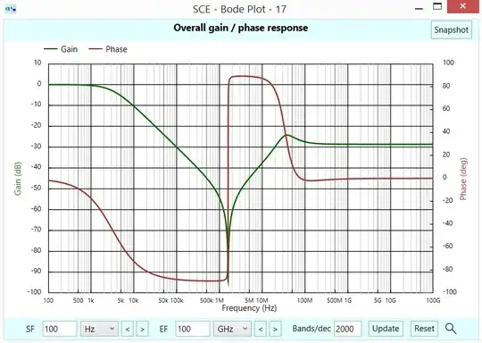
What can you measure & learn from this photo?

TL:DR

Mods ;) feel free to edit

In transformer currents, ringing is a sure sign of 5th order effects from saturation current or over-voltage.

More harmonics

My Law of Harmonics are expanded:

EVEN harmonics are caused by any amplifier as tubes, FETs and BJT's are quadratic devices.

Yet perfect symmetry of square waves cancel all even harmonics. Duty cycle errors from 50.0% can be easily measured on a Spectrum Analyzer by correlation with 2nd harmonic distortion..

Vbe & Vgs control the output current with 2nd order curves unless there is feedback to reduce the modulation. ( degeneration and negative feedback )

Clipping can generate all harmonics (unless perfectly symmetrical which is rare)

In complementary logic devices duty cycle of logic can be easily and precisely measured by the 2nd harmonic ratio on a spectrum analyzer.

Pulse asymmetry is due to the imbalance of RdsOn or unequal prop delays in an XOR.

So the extreme case of a narrow pulse has all harmonics up to the 1st missing harmonic equal to the resonant frequency of a parasitic LC circuit or the gap wavelength of a repetitive arc in MHz triggered by Grid or RADAR rates.

Pour s'amuser

http://www.falstad.com/fourier/

Tony Stewart EE75
  • 1
  • 3
  • 54
  • 182
  • Thank you Tony, I can see varying series resistance at the source will play very important role to avoid overshoot, but the problem for me, series resistance is not placed close to the source but somewhere in between. – AKR Mar 17 '22 at 09:14
  • The problem for me is I modelled your results well but you have given no feedback on my assumptions nor any details on layout or components. Yet I have more than fully answered your question with why ringing occurs and some ways to prevent it – Tony Stewart EE75 Mar 17 '22 at 14:06
  • Your assumptions are very close to my circuit, and thanks again for the explanations, just waiting if incase some other experts want to add to the topic before I mark it as correct answer. – AKR Mar 17 '22 at 15:09
  • 1
    Ask @Andyaka he's good or even better Spehro – Tony Stewart EE75 Mar 17 '22 at 15:30