1

I'm trying to design an electronic load that will take DC or AC (up to 20kHz, for audio amplifier or bench power supply testing) and show a constant (but adjustable) resistance. I'll be using N-FETs back-to-back to dissipate the power, controlled by an op-amp to keep adjusting gate voltage to get something resembling constant-R. I want to avoid P-channel FETs as I have some N-channel power FETs available already.

I'm not an EE and have never used op-amps before. This is turning out to be much more difficult than expected. I would like to keep the complexity of the circuit low, as to no require designing and ordering PCBs.

The circuit: circuit

For positive halfwaves, things look ok. Negative halfwaves however drive the op into the positive rail. The sign is correct, but the value is wrong:

graph1

  • green: load voltage
  • blue: load current
  • red: op output with respect to its separate ground

If I swap the op inputs, the result for the negative halfwaves looks more reasonable (but are crooked and offset): graph w/ swapped op inputs
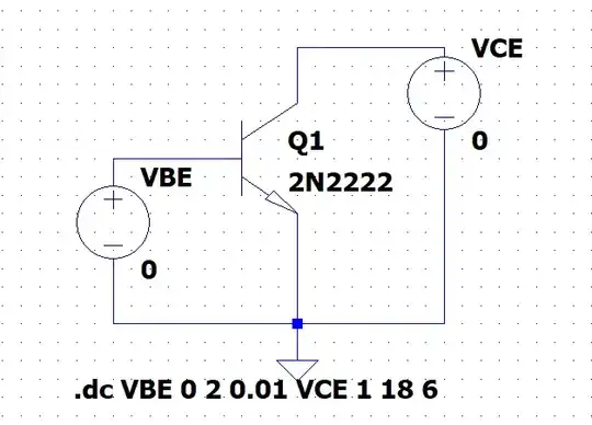
I'm at a loss what to do now. Is conditionally swapping the op inputs possible? A good idea? Even if I did that, it still looks wrong.

I considered just using a bridge rectifier to get a simple-to-handle DC load, but the diode drops would make the load very non-linear at low voltages. While there are ideal-diode bridge rectifiers like the LT4320, they top out at 600Hz, and presumably expect a constant frequency.

Is there a better way to do what I want?

What's the best way of minimizing the current peaks during zero crossings? Naturally I want the OP to recharge the FETs quickly, but not start oscillating.

devnull
  • 8,447
  • 2
  • 15
  • 38
1N4001
  • 163
  • 6
  • Think about what's going on with R1 - there will be an AC voltage across this with a 0VDC reference. So say +/-100mV. What happens if you input -100mV into an opamp which is only powered from 12V and 0V? – rdtsc Mar 06 '22 at 20:13
  • @rdtsc The opamp never sees a negative voltage differential, the positive input is also hooked up to the load specimen. – 1N4001 Mar 06 '22 at 20:22
  • Actually you're partially right. It's not that simple. Which is why I think I need to conditionally swap the op's inputs for this to work. – 1N4001 Mar 06 '22 at 20:32
  • 3
    Why not full-wave regulate the signal and make the circuit operate in one quadrant. Sure there'll be some cross-over distortion but now, you've reduced the problem to something that maybe a moderate power op-amp can deal with without using a MOSFET. – Andy aka Mar 06 '22 at 20:42
  • @1N4001 with the op-amp Vee grounded, and V1 on that same ground, then R1 *will* be going +/-100mV while the op amp Vee is still 0V. This is "beyond the rails" and most op-amps can't deal with it. – rdtsc Mar 07 '22 at 16:16
  • 1
    Hint: power the opamp Vee rail from -5V. – rdtsc Mar 07 '22 at 21:13
  • @rdtsc Gave that a try, just to see if there was something I didn't consider. To my lack of surprise, the op still slams the output into the *positive* rail. – 1N4001 Mar 07 '22 at 22:43
  • What LTSpice opamp model are you using? – devnull Mar 07 '22 at 22:52
  • @devnull I've been using the generic `UniversalOpamp2`. Now I realize this was a mistake. Regulation breaks when I replace it with an actual opamp model, such as an LT1677. This is becoming hopeless... EDIT: Found a spice model for the common LM358 and loaded it in. Also breaks regulation, on top of lowering sim speed by a factor of 1000. – 1N4001 Mar 07 '22 at 23:35

2 Answers2

2

Here is a crude idea you or other members may want to evolve: what if the fact that the opamp saturates in one semi-cycle is used to make the circuit "work"?

Starting with some problems/comments:

  1. Assuming that shunt voltages can be kept low enough so that the opamp outputs applied to the gates can compensate as the current increases in the shunts moved between the sources and the reference
  2. Assuming you can "float" the signal source, so the same reference can be used for current measurement, gate voltage and opamp power supply
  3. The actual "simulated resistance value" will have to be trimmed separately (R2 and R4) since the lower voltage measurement will vary all over the place as the MOSFET temperatures vary
  4. High frequency will obviously not work with such simple arrangement (again, this is just a concept)

This ugly option was implemented as you mentioned a low component count is important. If you can use differential amplifiers that can handle the common mode voltage to sense source current and voltage you could overcome the problems with gate voltage limitation and dependency of the \$R{ds(on)}\$.

enter image description here

enter image description here

If you think this is worth trying, you could develop it further and post specific questions later to avoid broad discussions and allow contributions to solve specific problems.

But I still wonder why a box of power resistors would not do the job.. ;)

devnull
  • 8,447
  • 2
  • 15
  • 38
  • 1
    I think it's more efficient to have transistors mounted on a heatsink, than resistors, and "power wires" (NiCr & co) bring their own inconveniences. – a concerned citizen Mar 11 '22 at 15:08
  • 1
    @aconcernedcitizen Indeed. And the active one is a very interesting problem to solve. Very low input offset requirements, accurately measuring currents with a 2~3 orders of magnitude with the same shunt, fast switching... I've failed to find AC solutions which were not targeted at 50/60 Hz and line voltages. – devnull Mar 11 '22 at 15:19
  • 1
    The efficiency is the same no matter what the dissipator is. Watts is watts. Some resistor packages, like some transistor packages, are designed specifically for heatsink mounting. And just like power MOSFETs, resistors come in TO-220 and TO-247 packages. Transistors get you continuously a variable load with no switching transients. Nothing more. – AnalogKid Mar 11 '22 at 16:15
  • 1
    Resistors do have a fundamental advantage in reliability compared to power transistors. Transistors are made to tolerate heat, while resistors are made to *make* heat. I don't think that matters in this application, but in others it certainly does. – AnalogKid Mar 11 '22 at 16:21
  • 1
    Thank you! This works great in my simulation. I really struggled to wrap my head around the separate grounds and relative voltages (and still do!). There remains one disadvantage with the separate gate drivers tho: Only one FET is conducting at a time, so you're relying on the body diode of the other. This is likely going to distort around zero-crossings. – 1N4001 Mar 12 '22 at 15:47
  • @1N4001 No. Both MOSFETs are conducting all the time. They switch roles at each semi-cycle: "controlled resistor" <-> "ideal diode". Body diodes never used (look at the Vg waveforms). – devnull Mar 12 '22 at 15:50
  • And as for why not use power resistors: An electronic control like this can be extended. I'm planning on adding a constant-current mode, and possibly constant-power too. – 1N4001 Mar 12 '22 at 15:50
  • Yes very useful. But a DC constant current load is much simpler as it takes a voltage as setpoint input and this "simulated resistor" take as resistor (trimpot?) as input. So, less convenient but yet very interesting. – devnull Mar 12 '22 at 15:53
  • 1
    'They switch roles at each semi-cycle: "controlled resistor" <-> "ideal diode".' Indeed, you're right. I was looking at the gate voltage plot wrong. This works well, thanks again. There's some overshoot I want to fix, but I'll open a separate ask for that. – 1N4001 Mar 12 '22 at 15:59
  • @1N4001 You are welcome. I'm looking forward to see this idea improved and very curious to put one together. – devnull Mar 12 '22 at 16:01
2

I use a single FET plus a bridge to control fluorescent lights, and it works well. Audio is a much smaller voltage, so the crossover area (where there is zero current) is a much larger percentage of the total waveform. The rapid change in current at the beginning and end of each crossover area can cause ringing in the speaker cone. Changing to Schottky diodes would help by shortening the crossover area. Still, I don't think running the load voltage through a diode bridge will give satisfactory results; but it is a clue to the solution.

Your circuit tries to drive the FET gates with a negative voltage (negative Vgs) during the audio negative half-cycles. Because both FETs are n-channel, what you want is to drive the FET gates with a proportional positive voltage during both positive and negative half-cycles.

To do this, add another opamp as a precision full-wave rectifier between the load voltage sample (R4-R5 node) and the current regulator U1.

AnalogKid
  • 16,865
  • 1
  • 13
  • 25