8

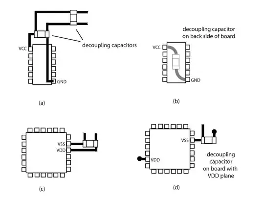
See this image which gives four options to place decoupling capacitors:

enter image description here

(from http://www.learnemc.com/tutorials/Decoupling/decoupling01.html)

I would say option (d) isn't good - I would recommend someone to place the capacitor near VDD instead of VSS. Is this right? The same goes for (c).

Generally: what's the best place to place a decoupling capacitor? Where would it have the most effect? And, more important, why? I'd like a theoretical explanation.

1 Answers1

7

Think of the copper tracks as series inductors. Series inductors are bad, you want them as small as possible. (B) is the better option.

Also loops in your tracks are bad, again they form an inductor and easily pick up (or radiate) an EM-field. You want the surface area of loops as small as possible, thus keep forward and return paths as close to each other as possible. (C) is the better option.

jippie
  • 33,033
  • 16
  • 93
  • 160
  • I guess you will be hardly argued (not by me, who am I?) over option (d) with the package in option (c), since the loop area is the smallest, as well as the track sizes. :) – abdullah kahraman Mar 14 '13 at 21:43
  • 3
    b might be better, but if there are no other components on the back of the board, it will do nasty things to production costs. – Scott Seidman Mar 14 '13 at 22:19
  • @ScottSeidman I sometimes solder a cap between the two rows of the chip socket. (I know it is production cost unfriendly too). – jippie Mar 14 '13 at 22:39