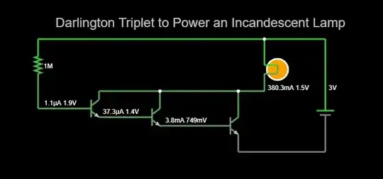
I was playing around in Falstad Circuit Simulator with powering a 2.5V incandescent lamp with a Darlington Triplet. I tried it two different ways and got slightly different results.
I'm not sure if either is technically correct, and I also don't understand what is causing the results to be different. This is just theoretical and I don't have a practical application for this, but I'd like to understand what is happening in each of the circuits.
I've tried to figure it out myself but it's beyond my beginner level. I'd really appreciate any and all beginner-level explanations. Thanks!
- 14,373
- 3
- 34
- 49
- 669
- 3
- 10
1 Answers
The difference in the two is related to where the first and second transistors in the triplet get their collector current. Your first circuit matches the description of what I would call a "darlington triplet", while your second circuit (with multiple emitters) would be better characterized as a cascade of two common-collector buffers (with the base as the only load) followed by a common-emitter amplifier/low-side switch
The important structural difference of the darlington pair/triplet is that all of the collectors are connected together. This allows you to consider the triplet as its own three-terminal device:
simulate this circuit – Schematic created using CircuitLab
Your observation of "slightly different results" is a bit ambiguous, but I'm assuming that you're talking about the different voltage across the load. Each BJT has a base-to-emitter drop of about 0.7 V (because of the forward-biased base-emitter PN junction), and a saturation voltage of around 0.03-0.3 (depending on collector current) V from collector to emitter:
As a result, the minimum voltage drop across this whole structure is around 1.5 V: two times a 0.7 V diode drop1, plus a saturation voltage for Q3. Thus, the darlington triplet looks like a BJT with a much higher current gain, and a saturation voltage of around 1.5 V (a downside).
You can look at this as a sort of feedback structure: If Q1 draws more current, it causes the voltage drop across the load to increase, which drops the voltage at Q3's collector, causing the voltage to drop at Q3's emitter, Q2's base, Q2's emitter, and Q1's base. As the voltage at Q1's base decreases, Q1 would draw less current. Note that in the triplet, Q1 and Q2 are in "forward active" mode, while Q3 is in saturation.
On the other hand, your other structure receives collector current directly from the positive rail for the first two stages:
Since Q3's emitter is now tied to the positive rail rather than the low side of the load, the load can now be driven with more current, until the voltage across Q1 reaches the saturation voltage. All three transistors can be driven fully on into saturation. This also means that the base currents are higher: Q2's collector current is 15 mA in this design (based on the simulation of the shown schematic) while the true darlington triplet only has 1 mA of Q2 collector current.
Note that in practice, this large saturation voltage for the triplet makes it annoying to use. Especially with low-power systems, excess voltage drops mean less headroom for useful signal swings. Wikipedia's article on the darlington pair reads:
A third transistor can be added to a Darlington pair to give even higher current gain, making a Darlington triplet. The emitter of the second transistor in the pair is connected to the base of the third, as the emitter of first transistor is connected to the base of the second, and the collectors of all three transistors are connected together. This gives current gain approximately equal to the product of the gains of the three transistors. However the increased current gain often does not justify the sensitivity and saturation current problems, so this circuit is seldom used.
1 This will vary based on temperature and the actual current. Q3 carries the least current while Q1 carries the most; if they were identical transistors then Q3 would have a modestly smaller Vbe drop.
- 18,062
- 2
- 47
- 73
-
2The second circuit could benefit from some series resistors, because otherwise it can have very large base current flowing through Q1. – jpa Feb 19 '22 at 07:31
