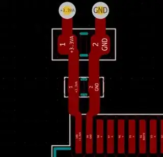
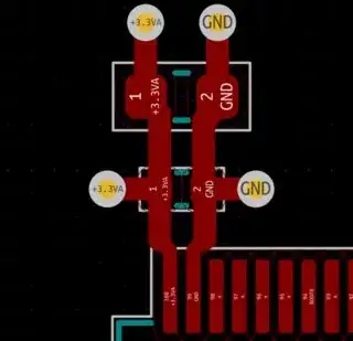
First of all, excuse my potentially poor understanding of electricity, I'm a low level programmer and I'm doing my first PCB (4 layer-stackup - signal/gnd/power/signal).
I was placing these two decoupling capacitors in parallel next to my microcontroller's power and ground pins (the bigger one is 1 µF, the other one is 0.1 µF) and I wondered :
Is it better to have only two vias as shown on the first image, so that current "must" flow through both capacitors before reaching the pin (and that's where I might misunderstand how current flows, maybe I have an understanding of it that is too "directional"), or should I also add two vias next to the 0.1 µF capacitor (second image) which I believe could reduce the parasitic inductance but makes me think that some current not filtered by the 1µF cap comes directly from the power plane through the 0.1µF cap to the pin ?

