9

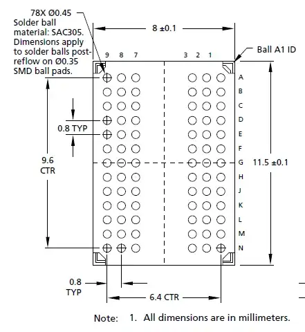
BGA DDR packages have a unique footprint. There are two columns of pads on both sides of the device, and an empty column in between.

enter image description here

Is there a reasoning behind the placement of these pads (in terms of PCB layout), or is this just a consequence of the design of the ddr3 silicon die?

More specifically, what I am wondering is, are there any tips/tricks/guidelines to place DDR modules on both sides of the board, directly across, or very close to each other?

SomethingBetter
  • 2,260
  • 7
  • 26
  • 33
  • I don't know, but I wouldn't be surprised if the footprint is patented and can be licensed (read: "payed for") by other manufacturers. – jippie Mar 13 '13 at 18:22

1 Answers1

6

You can take a look at a DDR3 die and Xray photo of the same chip here : http://chipworksrealchips.blogspot.com/2011/02/how-to-get-5-gbps-out-of-samsung.html

You can see that the memory is organized along a central spine and that the pad are placed along this spine. I can't tell you more about the internal layout as it's not my field of expertise.

For DDR PCB layout you can read this Application Note :

For the chips' placement it's more a signal integrity issue as the timings are sensitives. If your PCB and process technologies allows you any placement and your design is compliant with DDR/DDR2/DDR3 standard (mostly timing constraints) you are free to go with it.

I haven't seen a board with DDR3 memories for the moment, I only worked with a board with DDR2 chips. The five chips were placed on the same side (same or opposite side of the CPU) and side by side.

I can only recommend you to simulate your DDR design to be sure that your placement and routing are ok.

scary_jeff
  • 1,977
  • 8
  • 11
zeqL
  • 1,801
  • 10
  • 13
  • zeqL, the chip in your first link is actually a GDDR5 chip, not a DDR3 chip. – lamont cranston Jul 07 '15 at 21:13
  • It doesn't change the meaning of my answer :) GDDR and DDR are not so different after all. – zeqL Jul 08 '15 at 19:46
  • 3
    For those who came here later and the link to the "how to get 5 gbps out of ..." link, here is I think the original source: http://chipworksrealchips.blogspot.com/2011/02/how-to-get-5-gbps-out-of-samsung.html – hak8or Aug 08 '17 at 23:02