Your final question:
Does the first circuit make sense, or was a slight mistake in the circuit?
Short answer: As a conceptual potentiostat, both circuits seem to be conceptually correct to me.
Circuit one (for me) is not an educational representation and is a bit convoluted way to explain how a potentiostat works.
Other questions & answers were addressed along with this post.
Background:
About 20+ years ago, a friend of mine needed several Potentiostats for his Ph.D. research related to corrosion and some coating (paint) tests. At that time, these devices were prohibitively expensive (US$ 5K~10K) and he needed about ten devices! He asked for my help and I gave it a try, studying this "occult device", as seen by the Corrosion specialists, and built a working prototype for less than US$ 100.
I found your question, and the link you provided; then discovered this Texas' AN-1798 article describing something that may be useful for you.
With this background, I will explain how I see the matter and then your questions.
It will support the answers and contribute to demystifying this subject, at least for others in the EESE community.
Potentiostat Fundamentals:
Potentiostat is an electronic device that maintains the potential of a part of interest installed in the Working Electrode WE, when compared to a Reference Electrode RE.
This reference electrode is physically small and needs to be measured with a high impedance to not induce undesired polarization and bias effects.
The WE potential is achieved by controlling the current (Positive or Negative biased) from the Counter-Electrode CE (alternatively called Auxiliary Electrode AE) to the working electrode, in a closed loop.
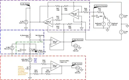
The specialist wishes to obtain data to plot the current as a function of the voltage in the specimen (WE). See the device setup and curve in the blue box on the following figure.
I will exemplify for electrochemical corrosion of metals now (I understand the case for bio-sensor can be slightly different).
If the metal specimen in the WE is made more negative, the cathodic current increases. If the WE is reversed, it will be more positive and this anodic current sometimes increases faster (higher slope - at least for certain alloy-electrolyte combinations).
It makes some sense to me that corrosion specialists see the current as their variable of interest, so they usually plot the current on the horizontal axis and in the log scale (it changes a lot!). Voltages are plotted on the vertical axis with a linear scale (see red boxed curves).
Electronically and mathematically, I would prefer to see the Current plotted (in the Y-axis) against Voltage (in the X-axis - green box).
The function I (V) also makes more sense to me, as the independent variable (of reference) is the voltage and the measured variable is the current. This is the plotting style adopted here (as in the last graph).
Potentiostat and Specimen simulation:
The conceptual diagram below (not so efficiently) uses "three" Op-Amp, but helps to explain how things work:
- Amp_A drives the current on the CE - either source or drain. If the current is large, it should be a Power Amplifier, driven as Amp_A.
The Op-Amp Amp_A2 receives the user input set-point and prepares it (inverts), while Amp_A is configured as a "Power" differential amplifier (Gain = 1000; low output impedance) comparing the desired set-point and the reference voltage from Op-Amp_B and tries to cancel any difference.
- Amp_B is a unit gain amplifier, to isolate the voltage from RE with a very high input impedance. It then buffers this voltage to be used in the input of Amp_A, or to be measured by the specialist, who confirms the Potentiostat has achieved the desired potential set-point.
- Amp_C measures the voltage drop in the shunt resistor (1 milli-Ohm), buffering and amplifying (G = 1000). The output voltage is equivalent to 1Volt / 1Ampere. Observe that with this configuration the voltage in the Reference electrode is NOT exactly at ground potential, as there is a voltage drop in R_shunt (R1).
- Electrochemical behavior of the Metal on Working Electrode is represented qualitatively with an Ohmic R_WE, in parallel with C2 (important for frequency sweep - not the case here), and the electrochemical non-linearities are represented by the modified parameters in one Zener diode component (V_direct = +0.7V; Vz = -0.1V R = 1 Ohm).
The working electrode (WE) is modeled inside the green dashed line, while the blue dashed line represents the complete electrochemical cell: WE together with CE, RE, and the electrolyte.
simulate this circuit – Schematic created using CircuitLab
When this circuit is simulated with a DC Sweep and using a Logarithmic scale, we get a similar "polarization curve":
About your questions:
On the first circuit you said:
I do not understand what happens at the B op-amp. It is a voltage follower, but I drive the bias voltage from my Vin to its output pin, like I force it to output a specific voltage. Why?
OpAmp_B simply buffers the potential of the Reference Electrode. Per the above explanations (including AN-1798), it is necessary to have a very high impedance (ideally zero bias current) to preserve the integrity of RE.
OpAmp_B is configured as a unit gain (non-inverting) amplifier. This is one configuration among several possible analog "operations" that can be done with an Op-Amp.
See a nice collection of amplifier circuits nowadays published by Texas - AN31 here.
"3. The current cannot go to V- of op-amp B, it will try to go inside the output of op-amp B", ..."
OpAmp_B has a very low ("zero") output impedance, so any influence of R1 or R2 does not affect the performance of Op-Amp_B (accepting push or pull of the current).
At first sight, I would not design a general-service Potentiostat with such low input impedance at R1 (110R) - but I don't know the article's specific details.
The important point is that Op-Amp_A is summing (with reverse polarities) the potentials of two sources. So Op-Amp_A is conceptually a differential amplifier:
- V_in = user set-point.
- V_RE = it is inverted (x -1) for Op-Amp_B and its output is also inverted!
How Amp_C is used is another point: It provides a virtual ground on the WE with a very-high transconductance gain (Rm = 29M - see next discussions of next circuit). I can only imagine the surface of the working electrode is quite small and requires diminutive polarization current.
"I later found another similar potentiostat circuit" - the second circuit
where you summarized:
- A1 takes input the Vin bias voltage, changes its output.
- A2 is just a voltage follower, gives feedback of the voltage from the RE of the postentiostat.
- A1 changes its output to match the feedback and the Vin bias voltage.
- Finally we measure the current with the op-amps at the vout (current to voltage converter A3, and a voltage follower A4.)
On this second circuit, as you said, we can observe:
- Amp_A2: An unit gain (buffer) amplifier for the RE.
- Amp_A1: The concept of a difference amplifier, subtracting the measured RE voltage from the Desired Set-Point, which is provided by the shown "Adjustable voltage reference". Observe that the amplification gain of the difference is NOT specified in this conceptual representation.
- Amp_A3: Is an Op-Amp that converts the input current to an output voltage. This kind of configuration is called transconductance amplifier.
Depending on the required current, this potentiostat has 2 (or 3) gain settings, selected by G1sw or G2sw (or both in parallel).
Also, observe that any Op-Amp wishes to maintain Vin+ and Vin- at the same voltage level.
As Vin+ = 0 in Amp_A3, this creates a virtual ground and allows to measure the WE current at ground potential.
This is better than my conceptual circuit, that I did NOT use a transconductance amplifier in the Amp_C exactly to show this issue. In real life this R_shunt disturbance might be negligible, but if the circuit could be improved, why not?
- Amp_A4: Is another unit gain buffer, to enable voltage readings of the WE current. Easier to interface with data acquisition systems.
Simulation tryouts:
As a general reminder, the circuit is a little more than "conceptual", as it can be simulated (link at its lower corner). I did not bias or selected the best Op-Amps or the most appropriate bias resistors, but the interaction capability of the shared circuit is more educative than just a conceptual circuit.
I would appreciate knowing your (and others') feedback.
. Euthymios


