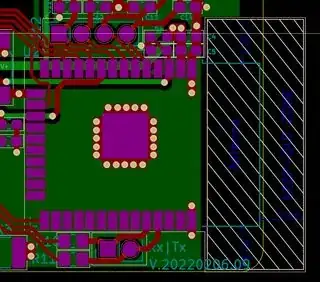
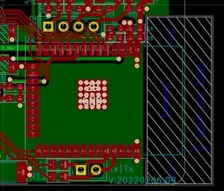
I am building my first PCB ever with an ESP32. I want the PCB to be built by JLCPCB (or similar) and I am not sure what to do with the Pad39
I read these opinions:
- Do not add vias in pad, and if you do put more solder paste in those pads (for example this post)
- JLCPCB can do vias in PAD (example link - but does not mention smt assembly)
- Official documentation says that Pad39 does not need to be solder at all
- Official schematics solders it and add vias to IT
Official docs (link to page 24):
Soldering EPAD Pin 39 to the ground of the base board is not a must, however, it can optimize thermal performance. If you choose to solder it, please apply the correct amount of soldering paste.
Official Esp32 DevKit Layout (I overlapped the layers) (documents link)
Do I need to do anything If I add vias before sending to JLCPCB/PcbWay? Would it be better if I add the vias outside to the pad? For example:
My full schematics and layout: link


