1

I designed a Arduino shield compatible board around the NXP LPC4337JBD144. so far I have been unable to get the first revision to program.

In the first design the JTAG header was not setup correctly, there were no bypass capacitors, the USB did not have all the pullups/pulldowns it needed, the DBGEN and TRST pins were not broken out to jumpers, and the Ethernet section did not follow spec as strict as it should have. I have able to add all the pullups to the JTAG and pull the DBGEN high and the TRST low by modifying the PCB with external jumper wires and resisters. I am still unable to program it with my JTAG.

I should note that the rev one PCB is only populated with what is necessary to get the chip programming and running, no additional hardware passive or active. I have tested that I am getting the correct signals from the JTAG and they are going to the right pins. I checked the crystal as well but I don't get a signal because the crystal will no initialize until the chip is programmed because the first thing that runs in a system configuration routine that sets up all PLLs and external oscillator settings. Everything on the first revision PCB has been check thoroughly with an oscilloscope, JTAG signals, crystals, and power section.

That being said I have been battling with this first revision for several weeks, I have tried everthing that NXP support has recommended, I have reviewed the schematics for several evaluation boards from NXP, Keil, and Hitex modifying my PCB along the way to bring it up to the ARM standard spec to no avail.

At this point I am convinced that the design is flawed in too many ways putting it way out of the standard specifications for an ARM Cortex M4 that it cannot be fixed with external modification to the PCB and that second revision of the design needs to be tested. This is a very time sensitive design, I was hoping to at least get the first one working then have the second revision be a fine tuning process. That being said I need to get a new design out to the fab house to keep my professors happy. I'm looking for constructive feedback on my new design, I have spent about two weeks looking through this design on my own and with the help of others in attempts to find anything that could be a serious potential problem down the road. I have been double checking the reference schematics and datasheet and I personally haven't detected any problems so far (most of my previous design work has been with AVRs).

EDIT: My board is 4 layers, the two outer layers are for signals and the two inner layers are a ground plane and a power plane. Right now I have the negative space on the two outersignals filled in with a ground fill polygon, could that cause some problems with the board such as ground loops?

Below I have attached the smart PDF for my Altium Project it includes the schematic and PCB design. https://www.dropbox.com/s/qb9ptr67v6msmh0/Abstract%20Hardware%20Device.pdf

Altium PCBdoc: https://www.dropbox.com/s/s7s0aw3yuh4va3g/Abstract%20Hardware%20Device%20PCB.PcbDoc

EDIT2: share link updated to Dropbox one. Altium PCBdoc shared.

Adam Vadala-Roth
  • 229
  • 3
  • 13
  • 6
    And what exactly is your question? Please read the [faq] on asking good questions. –  Mar 12 '13 at 19:02
  • I just want people to look at my design and point out anything that could be a potential problem. I've been staring at this design for two weeks going through the data sheet and schematics for reference designs making sure everything is perfect for this revision. I just don't want to have another board that doesn't work. – Adam Vadala-Roth Mar 12 '13 at 19:06
  • 2
    The link goes to a page with some obnoxious whining about browser version. There is no need for fancy features that are browswer-dependent when just trying to show us a schematic. – Olin Lathrop Mar 12 '13 at 19:10
  • You said the bypass caps were left off the board, but you don't mention them as one of the things you reworked. Trying to debug anything without proper bypass caps is pointless. – Olin Lathrop Mar 12 '13 at 19:14
  • The link had opened just fine in Firefox 19. There's a considerable design package at that link. – Nick Alexeev Mar 12 '13 at 19:14
  • 2
    @Nick: Yuk. I just want to see the schematic. A "design package" sounds like way too much detail, meaning the OP didn't spend time thinking about the information, just dumped it all here. It's not our fault nor our issue that this project is due tomorrow. Carefulness and attention to detail *saves* time, which may be why this project is in the situation it is. – Olin Lathrop Mar 12 '13 at 19:31
  • Its a PDF with the schematic. I did forget to mention it but I did add the bypass caps to the new design. Attempting to debug my first revision without bypass caps is pointless though? Is there a way I can attach a PDF to the post here? – Adam Vadala-Roth Mar 12 '13 at 19:32
  • If the first version has no decoupling caps, it will be horribly unstable (put a scope on the power pin of the device to see) – pjc50 Mar 12 '13 at 19:53

4 Answers4

15

When I review schematics/PCB during my day job, for a design like this, I would spend about 8 to 16 hours going over it. Clearly I cannot do that here. Further, I cannot give you a lesson in EE for each thing that is wrong in the design. And to make things worse, EE.SE is not really suited for a back-and-forth dialog that is normally required for a review like this. So here's what we'll do. I'll do a quick review of the design and put the issues that I spot in this answer. You read that, do some studying on your own, and if you still don't understand then you need to post a new question (not a comment on this answer). Here goes:

  1. You need some EMI filtering on the +3.3v to the center tap of the Ethernet transformers. Some sort of ferrite bead + cap(s).

  2. You need ESD protection diodes on the Ethernet signals to U4.

  3. 10 pF decoupling cap on X2 is astonishingly small. Use 0.1 uF.

  4. Ethernet termination resistors, R42-45, must be at least 0805's to handle the wattage required. I can't tell what size you are using.

  5. Something doesn't look right with the Ethernet TX CLK signal. I don't think you should have it connected to three chips (Oscillator, Phy, and MAC). Double check that in the Phy/Mac reference designs.

  6. Put a 0.1 uF cap on the "input" side of your ferrite beads.

  7. The note "crystal oscillator needs to be 12 mm away from the phy" is a HUGE red flag to me. It makes me think that something is not right, but I don't know what. If this were a normal design review I would grill you over this.

  8. You should filter or buffer reset signals that go over connectors (like SHIELD_RESET). This is a huge way for an ESD event, even 6+ feet away, to cause the PCB to reset.

  9. You should have a 0.1 uF decoupling cap(s) at every connector to reduce the AC signal return path for signals on the connector.

  10. It doesn't look like you have enough input caps on the DC power input. I could be wrong, however, since I can't read your schematics that well (stupid web-app).

  11. You might need more caps on the output of your voltage regulators. I didn't check, however, because I don't have time to read the datasheets.

  12. It is hard to really judge the PCB layout without looking at the design in the CAD software (Altium). But I see enough issues that the whole design needs to be scrutinized before being send out.

  13. Vias need to be spread apart so they don't cause slots in the power/gnd planes.

  14. Additional gnd planes on the top and bottom layers is not adding much to the design. It is worth it to just remove those.

  15. Do you have proper signal termination on the MII signals between the MAC and Phy?

  16. Have you verified that the PCB layer stackup is correct for the trace impedance you want and the signal termination that you have>

  17. You have signals crossing voids in adjacent power/gnd planes. This is a HUGE no-no.

  18. Your signal GND plane and your chassis-gnd planes overlap. Never, ever do this. (Disclaimer: I could be looking at the plots wrong.)

So there you go. Good luck!

  • Thanks for you very detailed and large response. This is exactly what I'm looking for, this is the right kind of feedback I need to learn and improve. That being said I did have some questions about the points you made and I have prepared the formal response but its too long to post. So I linked here on pastebin http://pastebin.com/hvquD42S – Adam Vadala-Roth Mar 12 '13 at 21:43
  • @AdamVadala-Roth As I said before, you need to do some research on each of these items and then if you have questions to post separate questions on this site to cover them. –  Mar 12 '13 at 22:17
  • 3
    +1 for a really detailed answer, unlike some comments whining about the links provided by the OP. – Anindo Ghosh Mar 13 '13 at 01:31
  • Upvote, but #4 not followed by everyone. See pic32 starter kit for deviation. – Erik Friesen Dec 26 '13 at 04:31
3

I popped open your board file. Lots of issues:

  1. You have rooms everywhere, and they're all enabled, and you're not using them. This is making everything show up as a DRC error. If you're not using them, turn them off.
  2. Once you turn off the rooms, you still have LOTS of DRC violations. You need to build a sane set of design rules. Generally, you go look up the capabilities for your board-house of choice, and build a set of rules around those. Err on the side of conservative minimum trace width/spacing, if possible. Just because $Expensive$ board house A can do 5/5 trace spacing means it's a good idea. 8/8 (8 mill minimum trace width, 8 mil minimum trace-trace spacing) is a good starting point. If you have really high density parts, you may need to go to 6/6
  3. It looks like you've drawn some of your own component footprints. It's good that you're learning, but you really need to look into adding proper 3D bodies to your parts. Right now, you have component-component collisions, because the RDC engine is using plain bounding-rectangles for component intersections errors.
  4. Your keep-out error on the USB connector is intersecting with the pads on the same connector, generating errors.
  5. I don't see any bypass caps for the micro on the PCB.

More stuff if you want me to keep looking

Note. Looking through the schematic PDF, it looks like the board file you provided is dramatically different then the schematic/board-overlays in the PDF?


On the schematic:

  1. STOP USING NET-LABELS: enter image description here
    enter image description here 
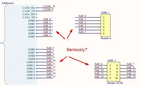
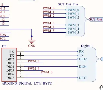
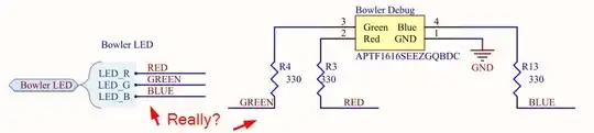
As a rule, net-labels make schematics harder to read and maintain. There are a few, specialized situations where they are beneficial, and if you don't know what those situations are, you don't have one. This is not one of them.
  2. Randomly oriented power-ports and ground labels: enter image description here
    enter image description here
    enter image description here
    Ground ports should always point down. Power ports should always have the text on the top (except negative rails, but you don't have any here).
    There are rare occasions where breaking these rules can be warranted.
    If orienting your power connections properly means you have to rework your schematic, do it. It will almost invariably result in a better, more readable schematic.
  3. Text over wires and parts: enter image description here
    Should be pretty self-explanatory. Just don't do it.

Crap that annoys me, less important: enter image description here
You have your schematic grid turned off here. Look at the connections to pin 1 and 4.
Turning off the grid makes it very easy to make schematics that look correct, but aren't actually connected.It also makes for sloppy, hard to read drawings. As a rule, in altium, everything should be on a 10-unit grid. If this means you have to patch your schematic libraries, do it. You'll be grateful later.

Also, you have a power port that's not quite on the end of a wire. Look at the dot on the ground port. This isn't such a big deal, but it is the sort of crap that would bother me.

Connor Wolf
  • 31,938
  • 6
  • 77
  • 137
  • Thankyou for your long and thorough response! I'm working on cleaning up the schematic right now, I did let it get pretty disorganized and sloppy as I moved through revisions. I modified the design heavily as I went hence the poor state of the schematic. As for the bypass caps they are there, the are the 100nF caps that pulled to ground on all the 3.3v inputs on the LPC4337, if I am mistaken and that is not the correct protocol for bypass capacitors I would like to know why I am wrong. Thanks again! I'll report back here after I have made heavy revisions. – Adam Vadala-Roth Mar 13 '13 at 05:43
  • In which situations do you recommend using the net labels? – NickHalden Mar 13 '13 at 15:38
  • @NickHalden - Honestly, that's something of a point of contention. Personally, I honestly would say "never". I don't use them myself, and I've done some fairly complicated multi-MCU drawings. I don't think anyone would say "all the time", but after that it really becomes a religious issue. – Connor Wolf Mar 14 '13 at 09:21
  • 1
    I think the best answer is "Only when they make a schematic more readable". *When* they do so is more of a matter of opinion, though it's **never** "often". – Connor Wolf Mar 14 '13 at 09:22
1

This is the datasheet for that part.

0) Are all of your power supplies and decoupling caps correct?

1) ARM JTAG is conventionally done with a 20-pin connector: http://www.jtagtest.com/pinouts/arm20 ; you have a 10-pin one and I think you may be confused between JTAG and SWD.

2) I'm skeptical of all those pullups and pulldowns, and that TRST isn't connected to the programmer. There is also a mystery 10k resistor in series with it.

3)Have you got the right JTAG clock rate? Do you need the return TCLK for the programmer (this may help with timing issues)?

4) Do you know that your programmer works and is configured correctly? e.g. do you have an eval board for this device that you've tested it with?

pjc50
  • 46,540
  • 4
  • 64
  • 126
  • 1. This is the page I am referencing also the design I linked in my pastebin writeup above on David Kessner's post. http://www2.keil.com/coresight/coresight-connectors 2. You can use either the reset or the TRST for the Cortex-M JTAG header,they both work most designs using the 10 pin connector utilize the rest and most 20 pin use the TRST. 4. It works fine I use it with my LPC4330-Xplorer evaluation board. – Adam Vadala-Roth Mar 12 '13 at 21:53
  • http://www.element14.com/community/solutions/7058/l/nxp-lpc4330-xplorer-schematics this one? That doesn't have pullups on the JTAG. I checked on my own design with ARM JTAG (different part though) and it had 220k ohm pullups. I think they're either too small or not necessary. – pjc50 Mar 13 '13 at 10:15
  • I was explicitly instructed to add those pullup resisters by NXP technical support. They said it could be one of the reasons why the first revision is not programming. What I can do is leave them in the design and choose whether or not to populate them/try different values. Thanks for your time and helpful feedback! – Adam Vadala-Roth Mar 13 '13 at 15:11
0

If I'm reading this datasheet for the RGB LED correctly, it's a common anode part. However, the schematic seems to show the common pin connected to GND, which only works with common cathode LEDs.

If you connect that anode to 3.3 V, the datasheet implies that even if pull the cathode of the green or blue chip all the way down to GND, it may not be visible -- the forward voltage could be as high as 4 V.

Maybe that (common) anode of the RGB LED should be connected to VCC_5v ?

I usually see some buffer, such as a SOT23 DMN65D8L nFET, between a processor and a high-brightness LED. I'm a little amazed that the I_OH and I_OL and I_OHS and I_OLS characteristics in the "Static Characteristics" section of the datasheet for the LPC4330FBD144 suggests that perhaps it can drive 20 mA LEDs directly.

davidcary
  • 17,426
  • 11
  • 66
  • 115
  • Thanks for your helpful feedback! I sort of jumped the gun on the tricolor LED. I was having trouble finding a cost effective RGB LED so I just picked the cheapest one I can find and used it. I'll look into a lower powered common cathode model. Thanks again! – Adam Vadala-Roth Mar 13 '13 at 15:13
  • UPDATE: I took another look at the datasheet and I went and calculated the resisters to be 1k to run the LED at 5mA. I did this because the LPC4337 has a current sink of 6mA for GPIO, the common anode is now connected to 3.3v. My friend who uses a lot of NXPs says this should be just fine but I'm open to more suggestions. Thanks again! – Adam Vadala-Roth Mar 13 '13 at 16:29