6

We want to design a pcb module that should be soldered directly onto customer pcbs (exactly like ICs ect.)

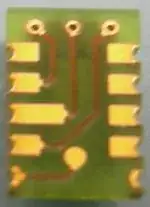
I found a module which does exactly that, please see pdf.

https://www.dropbox.com/s/ky2u9z83ja6snsh/pcb_pads.pdf

But how are these pads made i the pcb layout tool?

It looks like Plated through holes which has been placed half en pcb edge.

JakobJ
  • 2,298
  • 1
  • 21
  • 42
  • If your boardhouse does not support them and you only want to produce small series, you could also do full vias or through hole contacs and file one half of them away. This is what I did for the following PCB: http://nippey.dornuweb.de/index.php?art=13&page=3#thumb9 [Sorry for German ;] But I already guess, that this won't be a solution for you. – Nippey Mar 12 '13 at 07:24

1 Answers1

9

Those are called Castellated Vias, Castellated Holes, or half-holes, depending on what your board-house likes to call them.

Typically to have them in your design, you simply place a pad in the middle of your board outline route path, and then simply let your board-house know that your board has castellated vias.

If you want unusual pad profiles, you may need to draw up a custom pad shape as a special component.

enter image description here

Generally, if you have any questions, you should talk to your board-house to see if they can indeed do castellated vias, and how they want you to indicate them on the PCB layout.


See the electronics.stack-exchange question regarding Castellated Holes here.

Connor Wolf
  • 31,938
  • 6
  • 77
  • 137