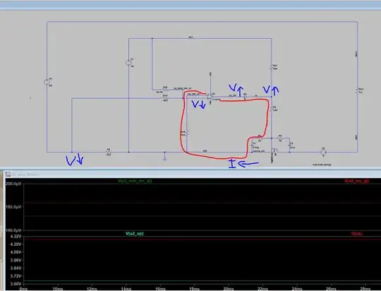
I don't see any kind of feedback in this circuit. Remember in any practical circuit, the power supply nodes (VCC and VSS) are driven by low-impedance sources, so the power supply nodes are not included in any feedback path. The inverting input IN(-) is connected to VSS through R18, so there's no negative feedback. And the non-inverting input IN(+) is connected to VCC through R28 and to VSS through R19, which makes a Thevenin equivalent source. So the op-amp doesn't even have positive feedback. There's also a diode in series with the output, which is unusual except for peak detect circuits.
Update: I misread the schematic (thanks @brhans). R19 is in series with R5. Visually I saw the entire lowest level horizontal wire as the VSS supply rail, I didn't notice R5. In spice simulations a value of 10m means 10e-3 or 0.010 ohm, which would be consistent with typical values for a current-sense resistor.
There's also another comment under the question, that seems to indicate I'm not the only person having some trouble following the intention of this design. Let me see if I can redraw it to better express the intention of R5 as a current sensing element. Note that I've placed R5 near the bottom, but slightly higher than the ground/VSS rail level, and I also routed the two sense lines close together on the schematic. When communicating with a PCB layout designer, this kind of detail on the schematic helps alert the PCB designer that these are a differential sense input, that needs to be routed close together.

simulate this circuit – Schematic created using CircuitLab
Rules and guidelines for drawing good schematics

