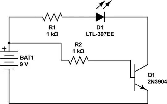
simulate this circuit – Schematic created using CircuitLab
Figure 1. (a) The NPN circuit redrawn. (b) The PNP circuit redrawn.
- In (a) the low-side NPN is driven hard and is fully saturated. As a result there is a very low voltage drop across it leaving most of the voltage available to the load.
- In (b) the high-side NPN is working in voltage follower mode which means the emitter tracks the base voltage with about 0.7 V drop due to the base-emitter junction. There is only 8.23 V available to the load.
For a 9 V, low-current application it works OK. If you were running lower voltage then the loss in available voltage may become a problem. If you're running a high current load then you will find it difficult to drive the PNP base hard enough without additional loss in base voltage. In addition, don't forget that you'll generally be driving the base from another transistor so there will be further voltage loss in that.
Note also that the power dissipated in the transistors will differ in proportion to the voltage across them. The low-side NPN is saturated so will dissipate little power. The high-side is not and will run hotter.
Low-side NPN switching is reliable, efficient, solves level shifting from the driving voltage to the driven voltage and is very flexible.


