0

I am testing a QSPI NOR FLASH device on a board I designed. It's datasheet is here.

Although it is working, I am seeing some glitches on the FLASH SDO (Serial Data Output) line. All other signals are inputs and look fine. I believe it is working because the glitch goes away before the clock edge.

It looks like the glitch is happening on a transition boundary, when the signal could switch from 1 to 0 or from 0 to 1 but won't.

I have attached a photo showing this. Any idea on what could be causing this?
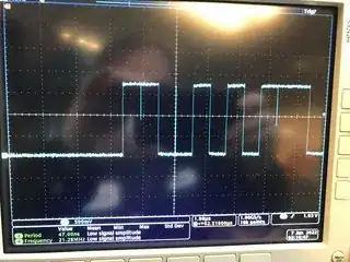
Glitch on Output Data

TonyM
  • 21,742
  • 4
  • 39
  • 62
Matty
  • 189
  • 5
  • 2
    Which specific QSPI flash device? Link to datasheet please? Other information such as supply voltage and to what is it connected to? – Justme Jan 07 '22 at 20:16
  • could be a design feature - what does the datasheet say? If you put a 100Ohm resistor in series, what is observed? Is it the QSPI flash that is glitching or the spi master - the 100Ohm resistor should allow that to be determined. It would've been helpful if your scope pic had SCLK as well. How wide is the glitch? – Kartman Jan 08 '22 at 02:07
  • 1
    Link to datasheet above. Datasheet doesn't say anything about glitches. The SDO line is driven from FLASH to voltage translator device (3.3 to 1.8) then to LS1046 processor (NXP) – Matty Jan 08 '22 at 20:06
  • @Kartman - glitch was measured at 9.6ns – Matty Jan 08 '22 at 20:07
  • 1
    Can you add the clock signal to your scope image? – Colin Jan 08 '22 at 20:08
  • @Colin - I do have a image but it won't allow me to show it - too large. I can say that the regular transitions are on the falling edge of the clock and then the spikes happen when a transition could occur. So the first signal above is a 1 for 2 clock cycles but the spike in the middle occurs right on the next clock edge. Hope that makes sense – Matty Jan 09 '22 at 00:03
  • @matty that does make sense, does the clock rise and fall cleanly, or is it glitchy too? Could the flash be interpreting a bump in the clock as an extra clock edge? – Colin Jan 09 '22 at 00:09
  • @colin good idea but clock looks clean – Matty Jan 09 '22 at 13:16

1 Answers1

0

SPI flash memories have an internal shift register or multiplexer to convert the internal parallel flash memory data to serial. In this case it looks like they have chosen to use a multiplexer. Multiplexers can have glitches on the output when switching to the next bit.

Glitches at clock transitions is completely normal in synchronous digital designs, and do not cause any problems. At most, it just adds a tiny bit of extra power consumption.

It is well within the SPI flash specification.

Timmy Brolin
  • 723
  • 4
  • 9