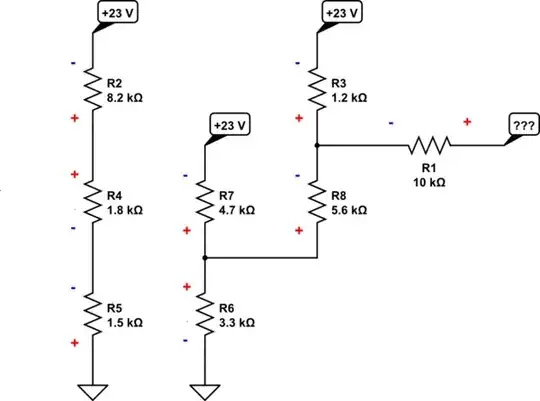
I tried solving this circuit using mesh analysis. I actually do not understand on how I can find the voltage in the open part. Moreover, the voltages of resistors in some loops are not summing up to zero. I am thinking that the given polarities affect in the computation. I have two concerns: where do I start to find the open circuit voltage? and what are the discrepancies of why voltages are not summing up to zero when plotting to KVL equations?

Asked
Active
Viewed 144 times
1
Sigwasan
- 29
- 3
-
3Please show us your equations. As for the R1, since no current is flowing through the R1 resistor. This implies that VR1 = 0V (no voltage drop across this resistor). So you only have three meshes to solve. – G36 Jan 06 '22 at 08:11
-
1The R2, R4, R5, V1 mesh is independent of the remainder of the circuit, and can be solved by Ohm's law – Chu Jan 06 '22 at 14:15
-
1We won't do your homework for you. You need to show us that you have made a substantial effort to solve this yourself. Show us all of your work, then ask a **specific** question. – Elliot Alderson Jan 06 '22 at 18:12
1 Answers
0
The very first thing I do before attempting to analyze a circuit is to redraw it. The process of doing it helps me think better and sometimes I also gather up a few details that I may not notice so easily, otherwise. But it also helps readability and tends to improve understanding.
Note that it takes lots of practice to accumulate a good sense about this process of redrawing schematics. But that practice is well worth your time.
Here's your schematic redrawn using rules I'll add as an addendum below:
simulate this circuit – Schematic created using CircuitLab
You get to call one node "ground." If you select a really convenient one, it can greatly simplify the analysis and reduce chances for mistakes, as well. (This doesn't always have to be the obvious choice or the one that the writer chose. You can move it to a different location if that helps you.) You should be able to see which node I chose, above. It's the negative side of the voltage source.
At this point, you should be able to see the independence of the loop involving \$R_2\$, \$R_4\$, and \$R_5\$. That loop has no impact on the rest. So it can be analyzed separately from the rest.
You should also be able to see that there are only two remaining KVL loops to solve, simultaneously. And since the current through \$R_1\$ must be zero, it follows that the voltage drop across it is also zero. So you don't need \$R_1\$ in the analysis of those two remaining KVL loops.
Finally, the sign arrangements for your resistors are unconventional. That's not a problem. The signs can be assigned entirely at random. But it does mean the problem is arranged to trip up some people who aren't being careful.
Redrawing Schematic Addendum
Rules to live by are:
- Arrange the schematic so that conventional current appears to flow from the top towards the bottom of the schematic sheet. I like to imagine this as a kind of curtain (if you prefer a more static concept) or waterfall (if you prefer a more dynamic concept) of charges moving from the top edge down to the bottom edge. This is a kind of flow of energy that doesn't do any useful work by itself, but provides the environment for useful work to get done.
- Arrange the schematic so that signals of interest flow from the left side of the schematic to the right side. Inputs will then generally be on the left, outputs generally will be on the right.
- Do not "bus" power around. In short, if a lead of a component goes to ground or some other voltage rail, do not use a wire to connect it to other component leads that also go to the same rail/ground. Instead, simply show a node name like "Vcc" and stop. Busing power around on a schematic is almost guaranteed to make the schematic less understandable, not more. (There are times when professionals need to communicate something unique about a voltage rail bus to other professionals. So there are exceptions at times to this rule. But when trying to understand a confusing schematic, the situation isn't that one and such an argument "by professionals, to professionals" still fails here. So just don't do it.) This one takes a moment to grasp fully. There is a strong tendency to want to show all of the wires that are involved in soldering up a circuit. Resist that tendency. The idea here is that wires needed to make a circuit can be distracting. And while they may be needed to make the circuit work, they do NOT help you understand the circuit. In fact, they do the exact opposite. So remove such wires and just show connections to the rails and stop.
- Try to organize the schematic around cohesion. It is almost always possible to "tease apart" a schematic so that there are knots of components that are tightly connected, each to another, separated then by only a few wires going to other knots. If you can find these, emphasize them by isolating the knots and focusing on drawing each one in some meaningful way, first. Don't even think about the whole schematic. Just focus on getting each cohesive section "looking right" by itself. Then add in the spare wiring or few components separating these "natural divisions" in the schematic. This will often tend to almost magically find distinct functions that are easier to understand, which then "communicate" with each other via relatively easier to understand connections between them.
- You get to choose exactly one node and call it "ground." If the purpose of redrawing the schematic is for understanding it, then choose a node that helps achieve that. When signals are single-ended, they share a common node and you should select this common node as "ground." If the purpose is for analysis, then you can select this for the purpose of reducing the equation complexity. Often, this will mean the node that is "busiest" (has the most terminals attached to it.) Either way, make this choice wisely and it will help a great deal.
The above rules aren't hard and fast. But if you struggle to follow them, you'll find that it does help a lot.
You can read a snippet of my own education by those schematic draftsmen at Tektronix who trained me by reading here.
jonk
- 77,059
- 6
- 73
- 185