4

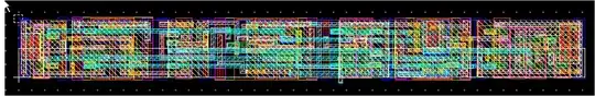
I'm following a discussion board that discusses an ASIC chip they are building, and they are using terms that I'm unfamilliar with. So far I've gathered

  1. Once a logic design is tested on an FPGA it can be ported to an ASIC with relative ease.
  2. The ASIC is created on a Wafer of ~1000 chips
  3. That wafer is chopped up into smaller chips called "dicing"
  4. "bumping"
  5. Packaging: (not sure what this means: "Aligning the substrates to the fiduciary marks")

As you can infer, I'm a little confused and overwhelmed by the process, but I want to get a handle on what is required and what the end to end process looks like.

Where can I find a detailed list of what happens after I test my FPGA logic and am ready to create several thousand ASICs based on that design?

makerofthings7
  • 523
  • 1
  • 4
  • 11
  • 2
    What specifically are you confused about? The actually fabrication process, or how to get to that point? Books have been written about each. – Matt Young Mar 08 '13 at 20:10
  • The alignment to the fiduciary marks basically centers the die to the center of the package. – Gustavo Litovsky Mar 08 '13 at 20:18
  • @MattYoung I'm simply confused because I made myself party to a subject I know nothing about and don't know where to begin. Books? do you have any in mind? I like the self-taught route via books websites or industry publications. – makerofthings7 Mar 08 '13 at 21:30
  • 2
    "can be ported to an ASIC with relative ease" - How do you define 'relative ease'? If you mean one guy in his garage, then no it's not relatively easy. If you have a team of 50 engineers and a few months/a year to do it, then yes. You are aware that fabricating a custom ASIC circuit costs millions of dollars, right? Here's a neat sheet with some cost estimates of the entire ASIC production flow. http://www.dz.ee.ethz.ch/?id=1592 – Tim Mar 08 '13 at 21:49
  • @makerofthings7 You've got (or will arrive to) an FPGA design, from which you might make an ASIC. Is that the plan? – Nick Alexeev Mar 08 '13 at 21:59
  • 1
    Answers on the following question are worth a read on some of the techniques and costs http://electronics.stackexchange.com/questions/7042/how-much-does-it-cost-to-have-a-custom-asic-made – PeterJ Mar 09 '13 at 00:36

3 Answers3

5

If you say you have a 'design ready on an FPGA', then I'll assume you have some verilog design which you have verified and tested on an FPGA. To get from here to an ASIC, you would go through the following (rough) steps:

Front End Design

  • The 'front end' of the design cycle generally includes writing of the RTL, and the synthesis of that RTL into a gate level netlist. I'll assume you are starting somewhere in the middle of this.
  • Once you have the RTL, you need to run through the synthesis flow, which converts your RTL into a 'gate level netlist'. An example of software used to do this might be DesignCompiler, by Synopsis.

Back End Design

  • The 'back end' of the design cycle refers to converting your gate level netlist into a 'picture' of an ASIC that would be understood by a silicon foundry.
  • First step would be to run initial floorplanning and place and route, which is essentially picking where you want each gate in your design to be positioned in the IC, as well as figuring out how to connect each of these gates in a finite layer of wires.
  • At this point you might run timing checks (see: Synopsis PrimeTime) to make sure that your design meets your required clock frequency.
  • Once you have your design fully specified, then you need more software (ex. Cadence Virtuoso) which can export your design into the file formats understood by a foundry (GDSII, for example).

Fabrication

  • At this point, you have your GDSII in hand, and you call up a contract foundry like TSMC, negotiate with them, and then hand them several million dollars and your GDSII, and wait for 3-6 months. TSMC then takes your design, creates the layer masks, and etches several thousand of your designs into wafers, then slices the wafers up for packaging.
  • The ASICs at that point likely go to a contract assembly, where they will be bumped (solder applied to the pads on the bottom of the silicon for soldering to a package), and then packaged (the bumped chip will be attached to whatever kind of package you require, be that QFP, DIP, BGA, or whatever you need).
  • At this point your IC is packaged and ready to go, and will be shipped back to you.

There's also a lot of testing that goes on between each step here which I've mostly omitted. Also note that each piece of software mentioned here likely costs in the 6 figure range, and there's probably a few more that I neglected to mention.

Also as I mentioned in my comment, here's an informative excel sheet which gives a rough estimate of the costs of each step: http://www.dz.ee.ethz.ch/?id=1592

Tim
  • 1,316
  • 7
  • 14
  • It might be worth noting that for smaller chips and lower volumes, there is the option of using a multi-project wafer service ([Mosis](http://www.mosis.com) is one company that provides such a service). –  Mar 09 '13 at 01:41
3

The term ASIC means "Application Specific IC" which originally meant an IC with a specific function. Now a days ASIC really refers to a design flow of a HDL, Synthesizable HDL to RTL, P&R etc. as described nicely by @Tim.

So it should really be called"doing a design with an ASIC Flow" but confusingly people just say ASIC.

An ASIC flow can be targeted to a Gate array or standard cells. But gate arrays have not existed in process nodes below 0.5u.

Full custom refers to generating the GDSII (design layout description) or some other variant directly. This is called "polygon pushing".

But sometimes cells from the standard cell library are used and perhaps blocks of a full custom chip are described using a ASIC flow and routed and placed as a block in a reserved area.

Here is a snap shot of a D_FF layed out in a full custom flow:

  • all layers:

enter image description here

enter image description here enter image description here

Here FEOL = Front End Of LIne - implants and active area definition

Here BEOL = Back End Of Line - Metals and interconnects

4.8u high

placeholder
  • 29,982
  • 10
  • 63
  • 110
2

My knowledge of this area of electronics is limited, but I'll try to give you some overview.

Here's a pretty good video that provides an overview of the fabrication process. I think that will answer the fabrication part of your question

When it comes to getting a design to fabrication, it really depends on the fabrication house, which technology is being used, and how they operate. In general, there are four classes of ASICs: PLDs, gate arrays, standard cell, and full custom.

  • PLDs entail programmable devices such as FPGAs and CPLDs. The design cycle is shortest, but the per part price is highest at volume.
  • Gate arrays contain predetermined components and are are held in stock. What the designer ends up having control over, is the interconnect between the components that the array designer chose. The design cycle is longer than FPGAs, and the per part price is lower than the PLDs.
  • Standard cells give designers a library of parts from which to choose. Each fab house will have a different library. The part designer will choose from this library to make their own part. Since the designer has much more control of the actual masks than the gate arrays, these parts are often called semi-custom. These part will have a longer design cycle, and cost less per part than the gate arrays and PLDs.
  • Full custom parts are designed from bare wafers, with every single transistor placed by the designer. Since the design engineers have complete control, these parts offer the best performance. The design cycle is longest of all the ASIC classes, but the devices out perform the other options, and at volume, have the lowest price per part.

In general the design tools used for this kind of work are proprietary to the fabrication house, and won't be publicly available.

Matt Young
  • 13,734
  • 5
  • 34
  • 61
  • You suggest that full custom parts have the longest design cycle; for large parts, I would expect that would be true, but what if one needed e.g. a part that simply connected 32 pins together in various combinations using pass transistors, in response to signals on the other pins? If the design was such that figuring out where transistors and wires should go was be trivial, what else would be required? – supercat Jul 18 '14 at 17:55
  • @supercat I don't really have an answer to that. This is an area I've studied, but never commissioned a design. That application sounds like a good application of a CPLD, unless the volumes are enormous. – Matt Young Jul 18 '14 at 18:02