1

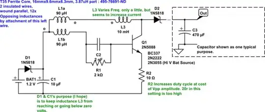
In this schematic is a simple blocking oscillator. Note that this won't simulate, as Circuit Lab does not have the type of toroid needed, but if you breadboard or prototype this circuit it will work fine.

schematic

simulate this circuit – Schematic created using CircuitLab

My modifications are clearly stated on the schematic. I've tried a variety of parts for each of these modifications but can't seem to find the right balance.

On a 1.8 V source, I get this result with the provided values in the schematic:

  • Edit: Frequency is in kHz enter image description here

A few explanations:

  • The Iout is a measurement taken by taking the voltage drop across a 10.4 ohm resistor across Out and ground over time, with the 470 uF electrolytic capacitor in place. I think that means (please forgive my math; read my profile to understand) 876.62 joules/μS. Please correct me if I'm wrong and point me to better math.
  • The 3 VDC beside Vpp is a DC bias created by R2.

Here is the oscilloscope image:

Oscilliscope Image

  • Edit: Oscilloscope shows 90 kHz in this image, but that changed 'FREQuently; it mainly stayed at 66 kHz

I am sure that somehow the frequency and duty cycle can be balanced better. Has anyone else found a way to modify it to be even better, or have suggestions to modify the one above a little more to improve the balance between voltage and current? I am aiming for a steady 12 V.

  • Edit: Thank you AndyAka. I don't understand about the component selection you mentioned in Circuitlab. I have gone through every component just now in Circuit lab in SE and cannot for the life of me find this component you are talking about. Which group is it in? How can I get it to act exactly as the toroid I hand-wound?
  • Also, you're right. I guess what I am looking for is a way to modify it, hopefully without wasting power through a Zener, balancing voltage and current to get just above 12 V, and efficiently drawing as much power as I can.
  • I have a very good use for this circuit and don't wish to discuss that portion here, but this circuit doesn't have much use because it's never really been modified to much good use, has it?
  • One good use I did play with while toying with ideas around it. I used the natural frequency of a similarly made circuit with a different toroid that produced about a frequency of 5 MHz and fed that through a transistor to drive the gate of a MOSFET. The AOD4186 MOSFET was set up as a typical boost circuit. It worked quite well. The 1.2 V source was able to produce the oscillation and amplify the transistor enough to drive the gate, though the duty cycle was poor.
  • Thanks to Antonio51 find cool ways to think out of the box and learn entirely new things. That sounds like it has potential, yes?
RobMcN
  • 165
  • 9
  • 1
    Get it running in your sim by using the features almost certainly (and simply) provided. Look for inductors and a coupler called "K". BTW you didn't mention what you are trying to achieve and this type of oscillator is not really practical in many situations. – Andy aka Dec 31 '21 at 20:28
  • @Andyaka Thanks for your comment. I've edited to fit your thoughts. I do have a complete soldered prototype that is working, of course. Just not as efficiently as I want it. – RobMcN Dec 31 '21 at 20:38
  • 1
    the emitter resistor is a source of inefficiency. You could try altering your transformer so that the output winding operates as a transformer rather than boost. Basically L1a/b form the blocking oscillator, L3 becomes a separate winding. You could replace D2 with a mosfet to save some lost energy. It comes down to balancing your various options for increasing one parameter vs the cost of achieving it. – Kartman Jan 01 '22 at 03:41
  • 1
    @RobMcN The whole success and performance of your converter depends on the voltage source. Without your voltage source characterised, engineering a solution would be chasing unicorns. One critical piece of information would be the cell impedance. For example 12V from a solar panel vs 12V from a lead acid battery are worlds apart in source impedance. Crafting a converter for a solar panel is a bit trickier than for a lead acid battery - especially when you're trying to optimise for best efficiency. I think that's the direction Andy is coming from. – Kartman Jan 01 '22 at 11:45
  • @Kartman thanks for the thoughts. I'm in hospital right now paralyzed from the waist down and don't know when I can try your suggestions. I'll get back to you. How do I find the source impedance (it is an uncharacterised/undocumented cell) – RobMcN Jan 06 '22 at 05:25
  • @Kartman By the way Kartman, How did you envision replacing the diode with a mosfet? I've tried a variety of options but not with great results, but maybe I'm not seeing what you are seeing. – RobMcN Feb 01 '22 at 17:08

2 Answers2

1

Something helpful ... Results of simulation.enter image description here

Efficiency. NB: Q2 is BFX34

Edit : efficiency = ~ 84% with K1 = 0.95 (nota : L2 deleted). Don't know yet if it could be better.

I added also a simulation with a stepping voltage power supply (from 0.8 to 1.6V).

enter image description here

If the input voltage supply is 1.5 V, efficiency is ~ 84 %, with output voltage a little higher.

enter image description here

Stepping Voltage power supply.

enter image description here

Antonio51
  • 11,004
  • 1
  • 7
  • 20
  • This and Kartmans answers are so interesting! Are these common circuits? There will be a long delay before I can try this (see my comment to kartman above) could you be so kind to implement the mosfet idea and describe the effect on a similar way that I described my result (freq, duty cycle,vpp, Vout)? Also what was the idea behind L4, C2? – RobMcN Jan 06 '22 at 05:33
  • 1
    Now, efficiency is more than 80%. Will try to implement with "logical level" mosfet. – Antonio51 Jan 06 '22 at 16:48
  • 1
    Idea behind L4-C2 is to keep source impedance for "blocking" as low as possible. As "battery impedance" is not know. Suppressed diode D1 (--> L4) because of "lost" on voltage of the diode. – Antonio51 Jan 06 '22 at 16:52
  • you're a genius. Using the toroid like that with a large capacitor to alter impedance. Nice. – RobMcN Jan 11 '22 at 04:59
  • Thank you for doing the extra work. It looks like I might be able to recover over the next couple of months and I'm eager to play with these designs in real time. Do you know if these are common modifications? Or have we made the community a bit better with some "joule-thief" modifications? – RobMcN Jan 12 '22 at 21:58
  • 1
    Take good care of yourself first ... The rest is "incidental". J-C. – Antonio51 Jan 12 '22 at 22:30
1

Circuit Lab does not have the type of toroid needed

Well, it won't have the "type", but what you have is a transformer. Whether it's a toroid or not doesn't matter much for the simple simulation.

It simulates great, and only needs a 1:3 transformer - both in simulation and in practice. With the core you used, that'd be 13:36 turns, to get about 50uH on the primary. I didn't add the leakage inductance to keep the schematic easy to read. It doesn't affect performance all that much.

schematic

simulate this circuit – Schematic created using CircuitLab

Q1 needs to have good enough gain. For lower gain transistors like 2N2222, a Sziklai pair needs to be used. Then the gain of the transformer can be lowered: a 1:1 ratio is sufficient.

schematic

simulate this circuit

This should perhaps let you explore more in the CircuitLab environment. It can be useful enough if you set things up carefully. It's not the most numerically stable solver, and has sometimes nasty transients that are entirely unphysical garbage, but with a bit of tweaking it can be made to do an OK job at least to explore the design space.

  • I actually enjoy your design with the 3 to 1 'transformer' and the sziklai pair. Is D2 used to bring Q2-base to ground each time? In both schematics, though, I do see large spikes that go into like -400V for the 2nd one and +100V (can't recall actually) for the first one. Would need efficient tweak for those. Thanks for the input – RobMcN Apr 01 '22 at 17:51
  • If the spikes are in simulation then they are just numerical junk. CircuitLab has real trouble with mixed time scales: if things go slow and suddenly they go fast, it has trouble getting it right. In a real circuit the avalanche action of the transistor will act as a C-E forward voltage limiter. D2 is there because while most transistors can avalanche C-E just fine without being degraded, base reverse breakdown can kill their gain. I haven't pondered about CE reverse breakdown much, I admit. – Kuba hasn't forgotten Monica Apr 01 '22 at 20:09