8

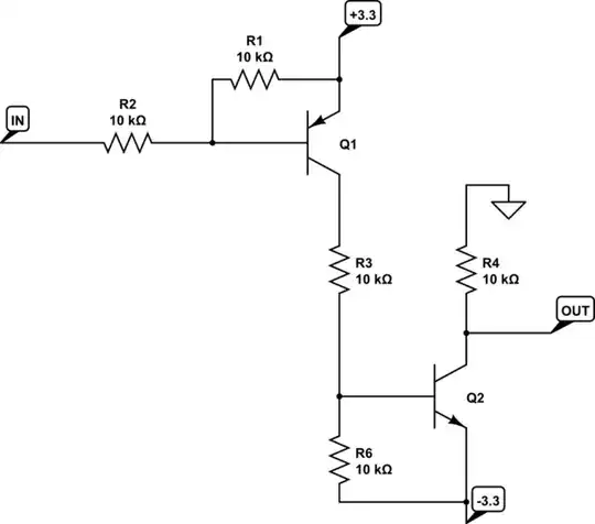
I have an RF switch chip that is controlled by a logic signal with levels of 0 V and -3 V. I want to control this from a CPLD that's producing ordinary +3.3 V CMOS levels.

Board area is at a premium in this design because I'm trying to wedge this in to an existing design.

Power consumption of a few mA or switching time as long as 100 us would not be a problem for this circuit. The RF chip's control input provides only about 10 uA load. Acceptable logic levels are within +/- 0.5 V of the nominal values. I can deal with either an inverting or a non-inverting solution. I have +3.3 and -3.3 V supplies available.

I have a "pretty good" solution to the level translation problem, but I'd like to know if there's a canonical "best" solution for this problem.

Edit

To clarify the output requirements, the output logic high needs to be between -0.4 and +0.6 V. The output logic low needs to be between -3.5 and -2.5 V.

The Photon
  • 126,425
  • 3
  • 159
  • 304

2 Answers2

11

This should be fine since you only need 100 µs response. With 10 kΩ output impedence, the 10 µA load will only cause 100 mV of offset, which is well within your spec.

Note that this inverts, so the CPLD output polarity needs to be adjusted accordingly.

Added:

I just noticed that maybe you only want 0 to -3.3V output, not +3.3 to -3.3 V. You mention 0 to -3.3 first, but then talk about ±500 mV as being acceptable, so I'm a bit confused. In any case, here is the 0 to -3.3 V output version. This one does not invert.

Olin Lathrop
  • 310,974
  • 36
  • 428
  • 915
  • Sorry that wasn't clear. The output logic high actually needs to be -0.4 to +0.6 V. The output logic low needs to be -3.5 to -2.5 V. – The Photon Mar 06 '13 at 20:37
  • @TheP: The bottom circuit meets those specs nicely. The high level will be around +300 mV and the low level not more than 100 mV above the negative supply. – Olin Lathrop Mar 06 '13 at 21:33
  • If your logic high could not be any more than 0.0V max (so -0.4V to 0.0V using his example), could you just increase the value of the emmitter resistor and it would work? – scuba May 07 '18 at 06:39
  • I thought more about this and realized my previous comment was misguided. Using something similar to what The Photon posted below would be more appropriate. – scuba May 07 '18 at 07:11
4

Okay, as promised, here's mine:

schematic

simulate this circuit – Schematic created using CircuitLab

As I mentioned in comments, it's excessively complicated, compared to Olin's. The only advantage this has is that the output voltage doesn't go above ground in the high state, which isn't even required for my circuit (but might be useful in another situation).

What makes it work at all, is using a complimentary pair with integrated bias resistors, like MUN5311DW1. This puts R1, R2, R3, R6 and both BJT's into a single SC-70 (2 x 2 mm) package, priced under $0.05 in volume (into the noise for my purposes). Under part number NSBC114EPDP6T5G, the chip can be had in a 1 x 1 mm SOT-963.

I think this circuit actually fits a slightly smaller footprint than Olin's, due to the reduced external discretes. Unless I can find a BJT with integrated emitter resistor.

Russell's idea of just using a zener and a resistor probably wins the footprint prize, but unfortunately I don't have the luxury of time to "play a little" to find the correct zener value on this particular project.

The Photon
  • 126,425
  • 3
  • 159
  • 304