0

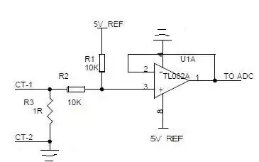
So here's the circuit and output voltage, the model is AD620:

enter image description here

So according to theory (Vout = 49400/49400 +1)*(2-1) ) i should obtain 2V as the output voltage.

Well what i got in LTSpice was a value around 2V with a lot of spikes, why does that happen? Also it doesn't hit the 2 V immediately. In the very beggining it appears to have some sort of transition.

Also from what i understood the reference voltage (taken from here https://www.analog.com/media/en/technical-documentation/data-sheets/AD620.pdf) is that it pretty much just defines the zero output voltage. What would happen if i change it to half of the value of the power supply?
Scipio
  • 773
  • 4
  • 8
  • 2
    Tip: Draw voltage sources with + on top, - on bottom. Ground symbols should point to the, um, ground. Some systems use upward pointing arrows to mean V+. It's not too important in this trivial schematic but good drafting makes the *schema* much easier to understand. See https://electronics.stackexchange.com/questions/28251/rules-and-guidelines-for-drawing-good-schematics if you're interested in developing your skils. – Transistor Dec 07 '21 at 19:32
  • 2
    All simulators, while capable of precisely simulating what they are programmed with, are *only an approximation* of real-world results. They will *never be perfect*, as such a model would be infinitely large and complex. Even the difference between properly-laid-out PCB and poorly-laid-out PCB can create as much variation (breadboards have even more parasitics - expect even more anomalies.) – rdtsc Dec 07 '21 at 19:54

2 Answers2

3

This is due to the finite numeric precision of LTSpice, it simply can't simulate your circuit more accurately than this. You can try setting an option for LTSpice to use double precision:

.opt numdgt 13

The more high-gain amplifier stages you add, the more these tiny imperfections in the simulation get amplified. The AD620 has a lot of gain internally to keep its differential pair accurate (A1+Q1 and A2+Q2).

If you see a (small) voltage spike at the beginning of the simulation, this is due to LTSpice being unable to compute the correct operating point of the circuit (again due to lack of precision). It then rapidly settles once the actual simulation starts as C1 and C2 in the AD620's internal circuit charge to the correct voltage. You can't really do much about this.

To address your second question: If you change the reference to half the supply voltage, then half the supply voltage will be added to the output voltage.

Jonathan S.
  • 14,865
  • 28
  • 50
  • With op amps that never happened, but i did what you suggest and now the output signal is constant but i still have nearly 2V in the very beggining for some reason – Scipio Dec 07 '21 at 19:36
  • 1
    The more high-gain amplifier stages you add, the more these tiny imperfections in the simulation get amplified. The AD620 has a lot of gain internally to keep its differential pair accurate (A1+Q1 and A2+Q2). – Jonathan S. Dec 07 '21 at 19:41
  • 1
    I've edited my answer to address your follow-up questions. – Jonathan S. Dec 07 '21 at 19:46
1

The AD620 has 120kHz GBW so 1ns startup simulations are inaccurate.

If you consider the noise BW for your gain, taking the noise figure enter image description heremay be estimated in uVpp enter image description here

Gain +1

enter image description here

Since the different pair front end is inverting into OA +/- inputs they become reversed and you now have two non-inverting inputs with each with gain 1 + AV for each polarity and Av is set by a common (shared) Rg value.

enter image description here

Here when REF=Vout=0 with 0 V diff. input.
Thus REF simply controls Vout offset. For single supply output into an ADC use REF = Vref/2 full swing about Vref/2 to the max input of ADC = Vref.

If your simulation only plots 1k points, be careful about Nyquist errors on the rise time of your step pulse for low bandwidth signals.

Tony Stewart EE75
  • 1
  • 3
  • 54
  • 182