I am reading the book Digital Design and Computer Architecture. In this book, it describes logic levels that map of a continuous variable onto a discrete binary variable. and it introduces two gates called driver and receiver. The output of the driver is connected to the input of the receiver.
Here is what the book says:
The mapping of a continuous variable onto a discrete binary variable is done by defining logic levels, as shown in Figure 1. The first gate is called the driver and the second gate is called the receiver. The output of the driver is connected to the input of the receiver.
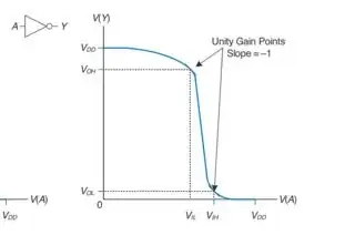
A real inverter changes more gradually between the extremes, as shown in Figure 2. When the input voltage V(A) is 0, the output voltage V(Y) = VDD. When V(A) = VDD, V(Y) = 0. However, the transition between these endpoints is smooth and may not be centered at exactly VDD/2. This raises the question of how to define the logic levels.A reasonable place to choose the logic levels is where the slope of the transfer characteristic dV(Y)/dV(A) is −1. These two points are called the unity gain points. Choosing logic levels at the unity gain points usually maximizes the noise margins. If VIL were reduced, VOH would only increase by a small amount. But if VIL were increased, VOH would drop precipitously.
My question is why we use NOT gate to build driver and receiver?
Is it aimed to amplify the signal? If it isn't, why not just connnect the output of a device to the input of the other device?


