1

Linked here contains the diagrams of the oscillator I'm referring to.

I'm confused about a few things:

  1. In the section showing the diagram with the freq register bits, this says "The input is taken from the data bus for the lower 16 bits while upper 8 bits are grounded." However there are only 8 values from the Data Bus (DB0 - DB7). I don't know if they meant "for the lower 8 bits while upper 16 bits are grounded" and accidentally switched the 16 and the 8, or if each value from the Data Bus is being used for two values in the freq register bits (making 16).

  2. Further down, in the section about the sum feedback of the oscillator, "The resulting sum is latched (inverted for odd bits) at sid_clk2" and I'm not quite sure what is meant by "latched." In the accompanying diagram, there are two different mosfets where the sid_clk1 and sid_clk2 lines are being fed into the gate terminal, but I'm not quite sure how this acting as a latch.

  3. At the top of the page before the diagrams: "Even bits have inverted logic to save some silicon and speed up the carry chain." I can see that even bits and odd bits are treated differently in the following diagrams, but I'm not clear as to why inverting the even bits is advantageous here.
Sez
  • 13
  • 2
  • 3
    Inline images please. Don't make people click a link and then have to flick back and forth between two tabs to see the context for what you're talking about. – Hearth Nov 21 '21 at 20:48

2 Answers2

2

Good one!, especially after I lost chess with my son twice in a row. Before starting, I am no where near from the chip design. So, please be generous before criticizing.

  1. In the section showing the diagram with the freq register bits, this says "The input is taken from the data bus for the lower 16 bits while upper 8 bits are grounded." However there are only 8 values from the Data Bus (DB0 - DB7). I don't know if they meant "for the lower 8 bits while upper 16 bits are grounded" and accidentally switched the 16 and the 8, or if each value from the Data Bus is being used for two values in the freq register bits (making 16).

The answer is in the main text:

The input is enabled by the $0 line for the low eight bits and $1 for the others.

The drawing does not explain, but implying $0 symbol still open the channel to DBx, meaning inverted. Thus the 8bit data bus is multiplexed between low eight bits and the others. enter image description here

  1. Further down, in the section about the sum feedback of the oscillator, "The resulting sum is latched (inverted for odd bits) at sid_clk2" and I'm not quite sure what is meant by "latched." In the accompanying diagram, there are two different mosfets where the sid_clk1 and sid_clk2 lines are being fed into the gate terminal, but I'm not quite sure how this acting as a latch.

I believe the drawing just contracted the latch, unless there are way to build a UJT like latch. Otherwise it takes some size to construct a latch, like this, this and that.
Otherwise, a bigger question arises about the latch. This stage can, possibly, avoid a latch, if the input registers and the last stage can latch. But the end stage must have a latch for V3_prev, but I do not see it. So, I insist :) that is contraction. enter image description here enter image description here

  1. At the top of the page before the diagrams: "Even bits have inverted logic to save some silicon and speed up the carry chain." I can see that even bits and odd bits are treated differently in the following diagrams, but I'm not clear as to why inverting the even bits is advantageous here.
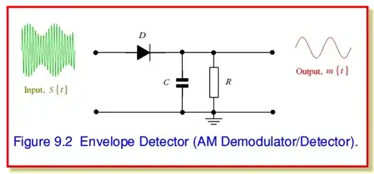
This part is hypothetical. I am lazy enough to ask you to do the logic expansion for me. An adder and the carry chain needs inverted input more than non-inverted ones on odd order (vice versa) in the carry chain.

jay
  • 3,781
  • 8
  • 24
0

For question 3 : your quote says "and speed up the carry chain" which is a big clue.

If the simplest logic inverts one bit relative to the previous bit, then you need to add an otherwise unnecessary inverter to restore the correct bit polarity. For example, NAND is simpler logic than AND - in fact the AND gate is usually a NAND gate followed by an inverter.

So if a computation can be done with a NAND gate instead of AND, you'll get a result (with the wrong polarity) faster.

If that logic is in the carry chain, that's 7 unnecessary inverters. So if you can live with alternate bits being the wrong polarity, you can knock 7 gate delays off the delay of your circuit, making it faster (as well as cheaper)