3

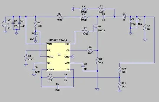
I am trying to design a SEPIC converter with the parameters stated above and have already drawn a schematic using the LM5022 IC. I have built the system and noticed a few things:

  1. The output voltage is a stable 19.66 V with an open circuit load, but the duty cycle of the signal that drives the gate of the FET is really small (~10% or less), while the calculations predict a 40-60% duty cycle as the input varies. I assumed that this is due to the schematic being calculated for a 0.5 A output current, thus I tried to test the system with such load.
  2. Placing a 40 ohm load made the FET instantly burn (it is rated for 1.5 A. MOSFET Datasheet) and the coupled inductors get really hot (they are rated for 900 mA. CM Choke datasheet) In practice, I am using a common-mode choke for the build (which I could not show on the schematic). I measure drain-source voltage peaks that could potentially exceed the FET rating (100 V). The inductor current at loads of 500-1000 ohms looks like short bursts instead of continuous triangle waves as is expected.

I am not sure at this point what other information to include, so please ask me anything I have missed.

enter image description here

EDIT: I have done simulations of the practical condition where my FET burns, Here are the first 2 ms of the ltspice graphs (I could not simulate the controller, thus am using a PWM to control the converter):

!!!One point, which grabbed my attention, the simulations spazz out if the PWM is at 5 volts, anything higher works just fine!!!

enter image description here

FURTHER EDIT!!! I have just build the SEPIC from the simulations without a driver controller and used a fixed duty cycle PWM to control it. It works impeccably. I probed all of the nodes with an oscilloscope, everything is almost 100% like in the simulations, which leads me to believe that the controller is not designed/working properly. The one thing that I do not understand about it is the compensation network, thus have not calculated the values for that and have put ones from the datasheet. Could anyone suggest an idea about that? (Thank you all for the valuable support up until now ^^)

I apologize for the ugly circuit
enter image description hereenter image description here

  • Are L1-L2 correctly coupled ? No reference + on terminals of inductor ? – Antonio51 Nov 11 '21 at 16:25
  • This is a pretty good question. Good job. I think you could make it even better by including the part number and manufacturer for the common mode choke and the transistor that is burning out. Do this by editing the question (not by replying to this comment.... I am going to delete this comment after you edit the question). If you are able to add a photo of your circuit, that will also help make it a better question. Sometimes the problem is something that you didn't think of at all, but which can be seen in the picture. – user57037 Nov 11 '21 at 16:58
  • Look at the pictures/oscillograms towards the end here: https://www.monolithicpower.com/en/how-to-avoid-inductor-saturation-in-your-power-supply-design – frr Nov 12 '21 at 09:24
  • BTW, taking a step back, your overall goal makes me ask you: would you consider some modern synchronous BuckBoost design? Try googling synchronous buckboost. I've seen the LTC3789 in several industrial PC's, never a problem with that one - except it doesn't meet your required upper bound on input voltage at 48V. But there are others, Google mentions LT8705, LM5176... I'd take a look into the relevant product categories (selector guides) with the implied manufacturers. – frr Nov 12 '21 at 09:55
  • I do not have the freedom to choose the design, A.K.A. SEPIC is mandatory ^^ – Yordan Aleksandrov Nov 12 '21 at 11:44
  • @Antonio51 I am not sure what this means, the inductors are wound on the same core, does their orientation matter then? – Yordan Aleksandrov Nov 12 '21 at 11:51
  • 1
    @YordanAleksandrov If there are coupled ... Yes, a"little" ... Just swap both ends of only ONE inductor. – Antonio51 Nov 12 '21 at 11:52
  • Oh no! CM choke used as two DM chokes. Please fix. – winny Nov 15 '21 at 13:38
  • @winny Is it bad to use a CM choke for this application? For the design I have included two options, one using a CM choke, and one that has separate inductors. I haven't tested the second one yet. – Yordan Aleksandrov Nov 15 '21 at 13:45
  • Yes, very much so. It will saturate immediately. Get yourself real DM chokes with enough saturation current for your worst case scenario with margin, and inductance in accordance with your calculations or manufacturer application note. – winny Nov 15 '21 at 18:47

4 Answers4

5

"the coupled inductors get really hot (they are rated for 900 mA.) "

Your inductors are saturating and the resulting high current spikes are killing the MOSFETs. The DC rating of a CM choke is typically well above the saturation if the currents in the windings are not matched.

Spehro Pefhany
  • 376,485
  • 21
  • 320
  • 842
  • I thought about that, but I am not sure what exactly happens when the inductor saturates, A.K.A. how those current spikes are generated as a result of it. Also, should I be expecting the current in the inductors to be larger than the expected output one? Because, currently the circuit draws much more current than it outputs, maybe due to the saturation? – Yordan Aleksandrov Nov 11 '21 at 17:17
  • Inductors oppose the current change - when an inductor saturates it appears like a short (more accurately, the DC resistance, which is close to a short). Yes, the peak and RMS current in the switch and inductors can, and frequently does, exceed the output current. – Spehro Pefhany Nov 11 '21 at 19:14
  • I second that. CM chokes are typically used for EMI suppression, which means two things: 1) the rated current is related to wire cross-section and resistive heat dissipation, but not so much to choke core saturation, as it assumed, that the DC currents flowing in the windings will mostly cancel out 2) the core material will be deliberately "lossy", which improves broadband EMI attenuation and dampens any resonant poles. Very bad for SMPS application. The OP should choose the right inductor for the job. – frr Nov 12 '21 at 09:14
  • A few years ago, I have seen a systematic manufacturing flaw in some Ethernet switch, where after some months or years of operation, some pieces would come back with smoke sediments around the toroidal inductor of the power input SMPS buck. Either the inductor was dodgy from the start, or the core got worse during operation for some reason (overheating making the material more lossy, leading to a runaway? not sure if this is possible). – frr Nov 12 '21 at 09:20
2

The chip drives your FET gate with 7V, so it'll turn on properly. However this FET is a bit wimpy with 0.25-0.3 ohm RdsON, and a tiny package that won't handle much dissipation.

It's a bit difficult to cool the FET here because vertical FETs sink heat into the drain, and here its drain is on the switching node where you don't want a large copper area. The datasheet specs a decent RthJA but it is with a very large copper area, which you don't have. So unless the drain of the FET is stuck right on the inductor pin and it uses the inductor as a heat sink, if you did a proper layout job and minimized the area of the switching node, then RthJA of this FET is going to be quite high. You could improve it by adding a few "thermal bridges" (ie, high value SMD chip resistors) between the drain and the ground plane.

Placing a 40 ohm load made the FET instantly burn (it is rated for 1.5 A. MOSFET Datasheet) and the coupled inductors get really hot (they are rated for 900 mA.

That's not coherent. A big inductor needs a while to heat up, so if the FET burned "instantly" then I'd say it failed short, which would short the switching node to ground so the inductor got the full power supply current. That means the inductors heating up may not provide useful information to diagnose the problem, it may just be a side effect of the dead FET.

Now since it's difficult to know what's going on, you need to probe it, and it's not convenient to probe a circuit that works for one second and then blows. So I would recommend powering this with a current limited bench power supply, set to just high enough current to deliver what you need for the test. Also replace the FET with something beefier, like a TO-220 with low RdsON, that will survive some abuse.

Then with this new FET the circuit will work long enough without smoking for you to actually probe it and figure out what's going on. Maybe it's inductor saturation, or just that the tiny FET gets too hot, or voltage spikes on the drain, etc.

bobflux
  • 70,433
  • 3
  • 83
  • 203
1

I saw no feedback connection from the output in the schematic. Maybe try to add it at first.

Null
  • 7,448
  • 17
  • 36
  • 48
QAM
  • 11
  • 1
1

Thank you all for the support! I finally made the SEPIC work and the issue was really the inductors. When I replaced those with ones that would not so easily saturate, the system worked flawlessly. Tips for others reading this and designing a SEPIC:

  1. Inductor currents can be much larger than output currents (depending on your application)
  2. Always calculate and choose suitable inductances as ones that are too small will fail to supply the required energy and provide your needed output. ^^